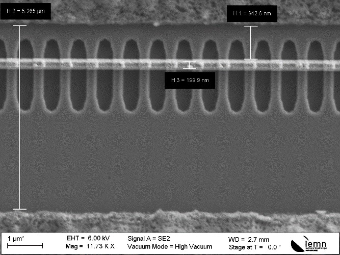
AlGaN/GaN high electron mobility transistor (HEMT) with a nanoribbon (NR) channel design permits to improve the transconductance linearity, reduce on-resistance (RON) and increase drain current density (IDS). The objective is applications in microwave and logic circuits.
The fabrication is based on top-down and bottom-up approaches. In the top-down process the nanoribbons consist of multiple parallel channels with nanoscales width made by etching (trigate structure) or by partial nitrogen ion-implantation isolation on the HEMT epitaxy. In the bottom-up approach, the nanoribbons are obtained by a localized regrowth of AlGaN/GaN epitaxy by MOCVD on a GaN/substrate after a resist deposition defining these nanoribbons.
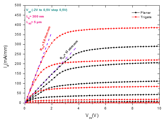
Devices with a gate length (Lg) of 300 nm and a source-to-drain spacing (LSD) of 5 μm were fabricated. A conventional device was also fabricated on the same epilayer for comparison. It is observed that the nanoribbons structure permits to reduce the access resistance, and thereby improve the device gm linearity. The electrical properties of the nanoribbon channel have been characterized by static measurement, and compared with similar conventional devices fabricated in close proximity of the epilayer. For a nanoribbon structure, it is observed an improvement of the current density compared with planar transistors. These results show the great potential of the planar nanoribbon GaN HEMT to be used in high linearity RF applications.
[1] BOUCHERTA M. et al, E-MRS 2018, Warsaw, Poland, September 2018.


