Selective area Molecular Beam Epitaxy of III-V nanostructures
Low electron effective mass materials such as In(Ga)As or InSb exhibit very interesting properties for different type of applications : high frequency/low power electronic devices (thanks to their low electron effective mass), infrared optoelectronics (thanks to their small bandgap) or quantum technologies (thanks to their large spin-orbit coupling). However, these materials also exhibit a large lattice mismatch with standard semiconducting substrates (Si, GaAs).
After several studies concerning strain relaxation mechanisms in highly mismatched systems and development of solution to reduce the impact of plastic deformation on the electronic properties of III-V semiconductors, we are investigating now the possibility of growing selectively these materials at the nanoscale. This approach has several advantages:
- promotion of the mismatch accommodation by confining the plastic deformation area at the interface with the substrate.
- reduction of the effect of different thermal expansion coefficients between the layer and the substrate.
- elaboration of nanostructures by a bottom-up way, thus avoiding surface degradation induced by dry etching.
If MOCVD is the most currently used technique for selective area epitaxy (thanks to the catalytic decomposition of precursors inside the mask aperture), Molecular Beam Epitaxy can also be used by adjusting carefully the growth parameters (growth rate, temperature, flux ratio) in order to promote the re-evaporation of III-elements from the dielectric mask. We have demonstrated that the use of an atomic hydrogen flux during the growth improves the selectivity for materials containing gallium or indium. Figure 1 shows the effect of an atomic hydrogen flux during the growth of GaSb on GaAs at 470°C.
![Figure 1 : Growth of 65 nm GaSb on a GaAs susbtrate covered with a SiO2 mask, without (left) and with (right) atomic hydrogen flux during MBE [M. Fahed et al, Nanotechnology 27, 50 (2016)] Figure 1 : Growth of 65 nm GaSb on a GaAs susbtrate covered with a SiO2 mask, without (left) and with (right) atomic hydrogen flux during MBE [M. Fahed et al, Nanotechnology 27, 50 (2016)]](https://www.iemn.fr/wp-content/uploads/2018/09/selective_area_molecular_atomic-2.jpg)
Figure 1 : Growth of 65 nm GaSb on a GaAs susbtrate covered with a SiO2 mask, without (left) and with (right) atomic hydrogen flux during MBE [M. Fahed et al, Nanotechnology 27, 50 (2016)]
This technique allows the growth of nanostructures of different III-V compound such as InAs, InGaAs, GaAs or InSb, particularly in-plane nanowires or arrays of interconnected nanowires as illustrated on figure 2. As the position of the nanostructures is well-controlled by the design of the dielectric mask, the devices can be processed easily without any transfer to a host substrate.
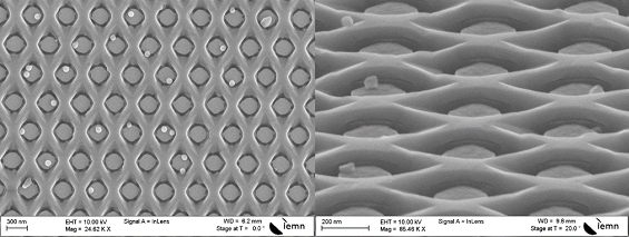
Figure 2 : Selective area epitaxy of an array of in plane InAs nanowires separated by GaAs nano-disks (top and bird view)
This approach paves the way towards the fabrication of new generation of in-plane nanowire based MOSFET, nano-tunnel diodes or ballistic nano-devices for quantum computation.
III-V heterostructures for HEMT, TFET and advanced mesoscopic nanodevices
The fabrication of III-V Field Effect Transistors, key components for electronic circuits working in the submillimeter wave range, relies on the epitaxy of heterostructures with an In(Ga)As channel associated either with AlInAs barriers or with an oxide. In this context, composite InGaAs/InAs channel has been developed for the fabrication of III-V MOSFETs during the MOSInAs ANR project (ANR-13-NANO-0001-01; coordinator: Sylvain Bollaert, IEMN; partners : LETI, LTM, IMEP, IEF, STM). Finally, InGaAs is also the material of choice as absorbing layer in uni-travelling carrier photodiodes (UTC-PD), pushing the cut-off frequencies of photodetection towards the THz frequencies (Figure 1).
![Figure 1: Schematic of the UTC device and SEM image of UTC-PD integrated with CPW [P. Latzel et al , IEEE Transactions on Terahertz Science and Technology 7, 800 (2017)] Figure 1: Schematic of the UTC device and SEM image of UTC-PD integrated with CPW [P. Latzel et al , IEEE Transactions on Terahertz Science and Technology 7, 800 (2017)]](https://www.iemn.fr/wp-content/uploads/2018/09/heterostructures1.jpg)
Figure 1: Schematic of the UTC device and SEM image of UTC-PD integrated with CPW [P. Latzel et al , IEEE Transactions on Terahertz Science and Technology 7, 800 (2017)]
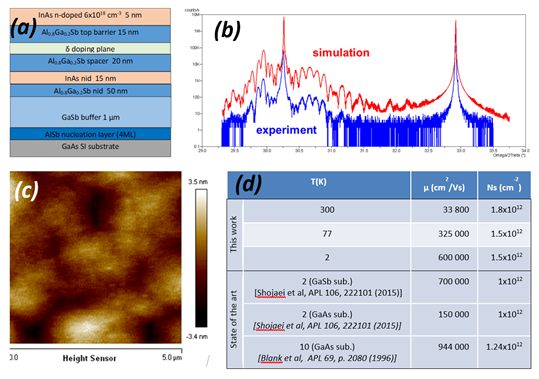
Figure 2: Structural and electronic properties of IEMN AlGaSb/InAs heterostructure grown on GaAs substrate
More than the high electron mobility, the wide variety of band alignments that can be achieved in the InGaAs/GaAsSb or AlGaSb/InAs systems offers many opportunities for electronic and optoelectronic devices. For instance, "Broken gap" or "near broken gap" heterostructures that can be obtained varying the Al content in AlGaSb/InAs heterostructure has been used for the fabrication of vertical tunnel FET with very high current density within the framework of the Samba ANR project (figure 3) (ANR 12 SAMBA JS0300801)
Moreover, the coupling between electrons and holes at the broken gap interface between InAs and GaSb quantum wells induced a hybridization of the band structure leading to the formation of a 2D topological insulator. In the frame of TOPONANO ANR OH Risque project (ANR-14-OHRI-0017-03; coordinator: Silvano De Franceschi, CEA INAC; partners: IN NEL, IEMN), nanoscale devices based on this concept are studied.Graphene on SiC studies
The growth of graphene layers on SiC substrates have opened the way to graphene nano-electronics. Graphene (an hexagonal plane of carbon atoms) may be described either as a metal with a vanishing density of states at the Dirac point or as a semiconductor with a zero band gap. Nevertheless, it behaves as a semiconductor for nanometric dimensions. Its planar structure (opposite to the carbon nanotube case) makes it compatible with usual microelectronics technologies.
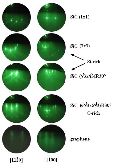
Two elaboration processes of graphene thin layers under ultra high vaccuum conditions are studied at IEMN. The first one involves optimisation of the 'standard' graphitization process of SiC substrates by high temperature annealing. RHEED is the preferred in-situ tool for characterization. Other techniques are almost systematically used, either in situ (Low Energy Electron Diffraction, Auger spectroscopy) or ex-situ (photoemission and Raman spectroscopies, atomic force and scanning tunneling microsocopies).
The second approach involves direct growth of graphene by molecular beam epitaxy, with a solid carbon source fitted into the epitaxial set-up. In principle, such techniques should be usable for various substrates able to sustain the required high growth temperature. For example, growth on sapphire results in a polycrystalline structure with nanometric domain size. The most striking results were obtained on SiC substrates, and more particularly on the SiC C face, within the european GRADE project ("Graphene-based Devices and Circuits for RF Applications", coordinated by M. Lemme, University of Siegen, Germany). In this case, the standard graphitization process is hardly controllable for mono to few layer thick graphene. On the C face, stacked graphene layers are twisted, as illustrated in the following figure.

Stacking of bilayer graphene on the SiC C face: Moire pattern for a 17.9° twist angle as imaged by scanning tunneling microscopy (left), corresponding scheme (center) and energy dispersion curve (the Dirac cone) for a ~2° twist angle (right), from Razado-Colambo et al., Sci. Reports 6, 27261 (2016).
Hexagonal boron nitride (hBN) and hBN/graphene heterostructure studies
Amongst its many exceptional properties, the two-dimensional (2D) material graphene is famous for its unusually high electronic mobility exceeding 105 cm²/V.s. But, whatever the way of producing the graphene, e.g. mechanical exfoliation or SiC high temperature graphitisation, very specific conditions are required to reach such high quality. In short, the graphene needs to be insulated from any external perturbation, whatever its origin (substrate, adsorbate...). This was achieved for example with suspended nanoribbons, or in rotationally decoupled thick stack of graphene. These solutions are not compatible with realistic devices, among many reasons because it is hardly possible to incorporate efficient gates in such geometry. Indeed, the electronic mobility of graphene in state of the art nanodevices is in the range of 103 cm²/V.s, which is far from these record values.
One solution to this problem has recently emerged, and involves another 2D material, hexagonal boron nitride (hBN). Because of its 2D structure, its roughness remains low, its surface is virtually free of dangling bonds and the charges trapped at the graphene/hBN interface only come in practice from foreign molecules. These latter tend to form clusters, which reduces the average scattering and results in high mobility graphene material (up to 14.104 cm²/V.s measured at room temperature) while retaining a quite high carrier density (~4.1012 /cm²) in hBN/graphene/hBN double heterostructures, the main scattering mechanism being phonon related. Hexagonal BN is a large band gap material (indirect band gap of ~6 eV), so that it can be used both as an insulator between the graphene layer and the substrate, as a dielectric layer between the graphene and the gate, and as a tunnel barrier in vertical transport devices. So, hBN is clearly an appealing solution to the problem of making devices exploiting the exceptional transport properties of graphene. Still, there remains a serious roadblock which is the need to make such graphene/hBN heterostructures by a scalable technique, a mandatory requirement when device applications are eventually targeted.
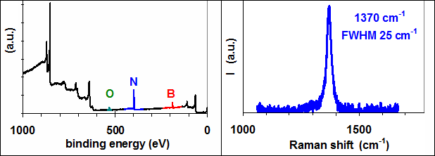
The graphene MBE chamber has benn equipped with a high-temperature effusion cell for boron, a RF plasma cell for nitrogen and a high temperature gas injector for borazine (B3N3H6. The final goal is to grow graphene/hBN heterostructures. The figures below illustrate the hBN heteroeitaxy on nickel.
Transition metal dichalcogenide epitaxy


![Figure 3: Vertical InAs/AlGaSb based Tunnel FET fabricated in the frame of the ANR JCJC SAMBA project and associated transfer characteristics [V. Chinni et al, J. Electron Device Soc. 5, 53 (2017) ]. Figure 3: Vertical InAs/AlGaSb based Tunnel FET fabricated in the frame of the ANR JCJC SAMBA project and associated transfer characteristics [V. Chinni et al, J. Electron Device Soc. 5, 53 (2017) ].](https://www.iemn.fr/wp-content/uploads/2018/09/heterostructures2.jpg)
