For two years, a new activity was started concerning the improvement of thermal management in GaN HEMTs since performance and reliability are strongly linked to this phenomenon.
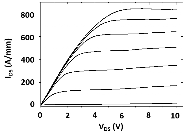
The first approach concerns the use of free-standing GaN substrate allowing homoepitaxy of the active AlGaN/GaN layers of HEMTs. The heat dissipation via the substrate is enhanced due to the absence of nucleation and strain adaptation layers which introduce thermal barrier. Technological process based on e-beam lithography was developed and first DC measurement was performed on AlGaN/GaN HEMT with LG=300nm (fig. 5a) showing the potentiality of GaN substrate.
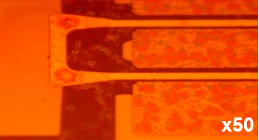
The second approach address the thermal management improvement of HEMTs thanks to a layer transfer technology on high thermal conductive substrate such as diamond. For that, the HEMT epilayer growth on silicon substrate is followed by device fabrication and bonding onto host substrate after the removal of silicon growth substrate. Technological process is under development with success to remove silicon substrate with limiting cracks in GaN layer (fig. 5b). Different bonding techniques are under study.
In the future, components operating at very high frequency (E,W bands) will be studied in collaboration with III-V lab. InAlGaN/GaN or AlN/GaN epitaxies will be considered on SiC, GaN substrates or reported on diamond. For this purpose, non-alloy ohmic contacts and/or self-aligned technologies will be carried out. The activity will be based on transistor processing, characterization and reliability tests for telecommunication applications.


