

According to the Copper's Law, wireless communication systems capacities have doubled every 30 months since 1900 and with a clear accelerated rhythm these last three decades where the capacity has doubled every 18 months. Needs and new services cover as of now many new aspects of our lives, as a result needs and exigencies are huge. THz solid state components whatever the functionality... amplification, detection, generation, systems... Whatever the device... transistor, diode, photodiode are in the centre of the future challenges. Anode group through its competencies in III-V technologies responds, faces, to this challenge.
THz High Electron Mobility and Heterojunction Bipolar Transistor
III-V technologies on InP substrate, making use of Indium and Gallium alloys, have shown their capabilities for high performance electronic and photonic applications, by demonstration of their superiority for high-speed communication and sensing. These excellent performances are related to the high mobility of III-V materials and possibilities of energy band engineering. This technology is considered for the next mobile network 6G where a high bit data rate of 100Gbit/s is targeted and is also at the heart of many THz devices. This data rate increase is mandatory to meet the growing demand from remote work, online education, shopping, entertainment, and recently by Internet of Things (IoT) needs. Indeed, the IOT will require the deployment of connected objects, whose number is expected to increase from 30 billions in 2020 to 100 billions in 2050. This is in this framework Anode group develops THz Transistors. The objective is to obtain maximum oscillation frequency FMAX beyond 1THz and to develop tools for measurements of this frequency. Preliminary result reports a FMAX around 1 THz on an InP-HEMT. Specific on wafer S-parameters characterizations were developed using multiline-TRL calibration technique up to 1.1THz.
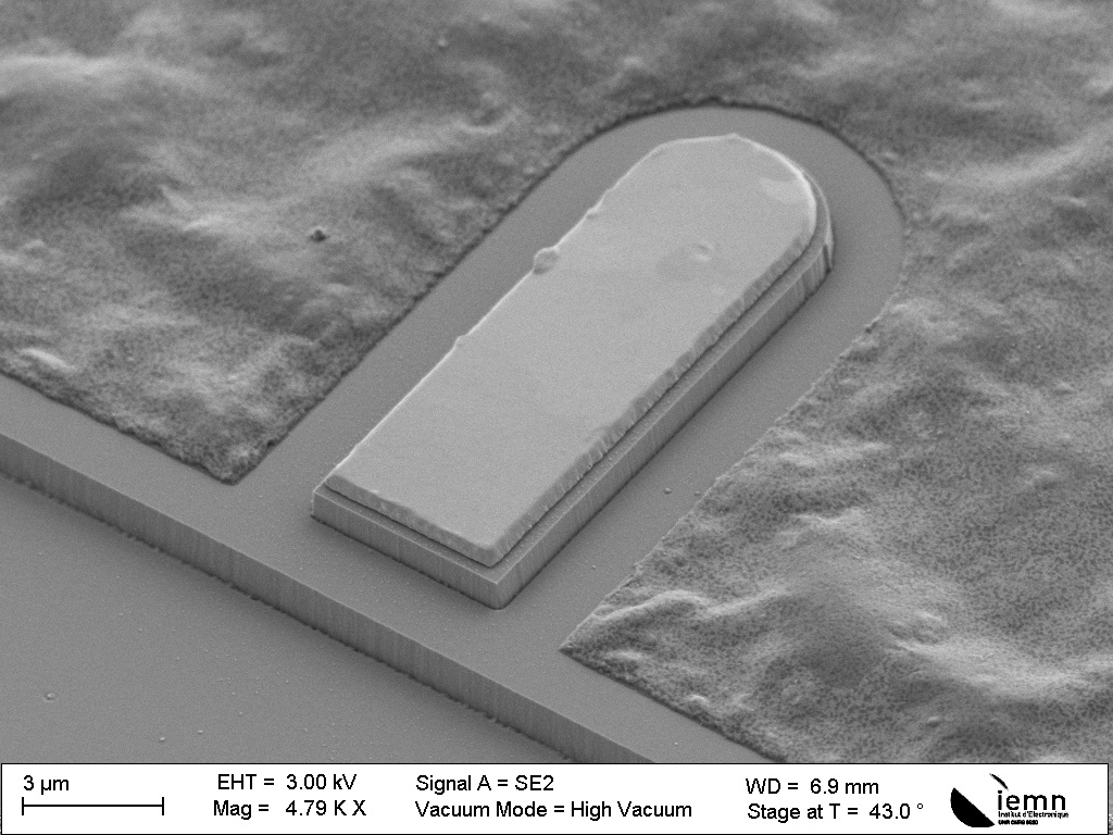
Concerning the HBT (Fig. 2), on an InP/InGaAs structure grown in InP substrate with a device area of 0.2×2.6 µm2the achieved performances are a FT of 350 GHz and FMAX of 650 GHz. In power at 94 GHz, this device delivered an output power of 12 dBm and P.A.E of 30%.

Fig. 1: 75 nm LG - AlInAs/InGaAs HEMT on InP Substrate

Fig. 2: InP/InGaAs HBT on InP Substrate.
GaN Schottky diode for THz generation
Frequency multipliers are solid-state devices widely used for signal generation in the millimeter wave range up to several THz. These sources rely mainly on the non-linear voltage-capacitance characteristic of a varactor diode. Traditionally, GaAs-based has been the cornerstone for producing these diodes dedicated to frequency multiplication.
However, recent advancements in III-Nitride (GaN) technology present compelling opportunities for enhancing the performance of frequency multipliers. GaN’s wider bandgap and higher breakdown voltage offer inherent advantages over GaAs, promising significantly higher output power—potentially surpassing current state-of-the-art GaAs devices by an order of magnitude.
We have collaborated with the University of Darmstadt, jointly supervising PhD student Chong Jin under the guidance of Prof. Dimitri Pavlidis. This collaboration has been instrumental in advancing our understanding and capabilities in GaN-based frequency multipliers.
Furthermore, our group has successfully secured funding from the French National Research Agency (ANR) for the SchoGaN project (2017-2022). This project focuses on developing GaN Schottky diodes tailored for THz generation. Currently, in collaboration with LERMA-Observatoire de Paris, our goal is to develop a GaN-based radiometer capable of studying the atmosphere of Venus under extreme conditions, such as temperatures up to 500°C.
Through these initiatives, we aim to leverage the superior material properties of GaN to push the boundaries of high-frequency and high-power signal generation, contributing to both fundamental research and practical applications in THz technology.
GaN Schottky diode
UTC for THz generation
In the framework of an IEMN internal collaboration with Photonique THz group, Anode group co-supervises PhD students since 2004. The scope of this activity concerns the generation of terahertz signals. The part of the electromagnetic spectrum - 100 GHz at 10 THz - is sorely lacking in compact, efficient and powerful sources. One possible way is the use of fast nano-photonics. UTC (Uni-Travelling Carrier) photodiode is a PIN-type diode where the optical absorption and the transport of the photo-carriers occur in two distinct zones, a p-type zone and an intrinsic-type zone. Photo-generated electrons in the p region diffuse to the intrinsic zone for collection. The technology of this device comes from that optimized for the HBT. Anode group has co-supervised a second and a third thesis and have been defended by F. Pavanello and P. Latzel.
Many technological aspects have been optimised (ohmic contacts, top metal contact, etchings). In particular, an original solution based on the concept of extraordinary transmission (Fig. 4) has been developed and allows a lighting from the top, much easier to perform. An RF power of 2 mW at 50 GHz and 400 μW at 300 GHz was measured on UTC-PD of 6 and 3 μm side. In addition, the state of the art in optical efficiency with 0.2% was reached at 300 GHz. In order to increase generated power, a transferred UTC process on a high resistivity silicon substrate has been developed to ensure a better heat dissipation. A strong performance improvement at 300 GHz was reported with 700 μW and an optical efficiency of 0.76%. This shared activity continues today through several ANR contracts and industrial collaborations (Rohde & Schwarz and RP GmbH). Our UTC is used for THz wireless telecommunication applications. Thus, in indoor, we have demonstrated for the first time of single channel 100 Gbit/s THz transmission in QAM- 16 modulation format. A fourth thesis is ongoing. The subject is "300 GHz signal generation for Wireless THz telecommunication". It is supported by DGA.

Fig. 4: UTC photodiode fabricated on InP substrate.


