


Three molecular beam epitaxy (MBE) chambers are running at IEMN. One is dedicated to III-V material growth, one to transition metal dichalcogenide studies. Both are coupled together with the ESCA analysis chamber under ultra-high-vacuum. The third one is concerned with graphene/hBN growth experiments. Two chemical vapor deposition systems are also available, dedicated either to the growth of Si and Ge nanowires or to graphene on metals.
Numerous characterization tools are also available, to give information about structural (X-ray diffractometer, atomic force microscope and scanning electron microscope), surface (ESCA), electrical (Hall effect) and optical properties (micro-photoluminescence and Raman), as well as two coupled thermogravimetry and mass spectroscopy analysis tools.
 All these equipments are part of Renatechthe french network of high-end facilities in the field of micro & nanotechnologies. They might be used to carry out research, by academia or industrial partners, national r international.
Growth
III-V epitaxy
A RIBER Compact 21 TM system, dedicated to the growth of III-V materials (Arsenides, Antimonides and Phosphides), is equipped with the following sources:
- III-element sources: Gallium, Aluminum, Indium
- V-element gas sources: Arsine and Phosphine with mass flow regulation and high temperature injector
- V-element solid sources: valved Arsenic cracker (Riber VAC500) and valved antimony cracker (VEECO Sb-200)
- Dopants: Silicon, Beryllium, Tellurium (GaTe) and Carbon (low temperature CBr4 injector)
- Atomic Hydrogen source: ADDON RF plasma cell
The system is cooled down with liquid nitrogen using a Vacuum Barrier set-up. Pumping is carried out thanks to a CTI OB250F cryo-pump and a 400l/s ion-pump.
In situ analysis can be performed thanks to the following tools:
- RHEED Staib 35kV (EK2035 type).
- a KSA system for RHEED image acquisition and treatment.
- a Hiden HALO 201 LC system for residual gas analysis
- an optical pyrometer together with a KSA BandiT optical absorption spectrum analysis for wafer temperature measurement.
This MBE system allows the growth of high quality III-V semiconductor thin films, 2D heterostructures for electronic and optoelectronic device fabrication and also of self-organised quantum nanostructures (quantum dots) or selectively obtained with respect to a nanostructured dielectric mask. The ultra-high vacuum environment and the wide variety of dopants ensure a very good control of the transport properties in the epitaxial layers.
This system is coupled under ultra-high vacuum to an XPS analysis chamber.
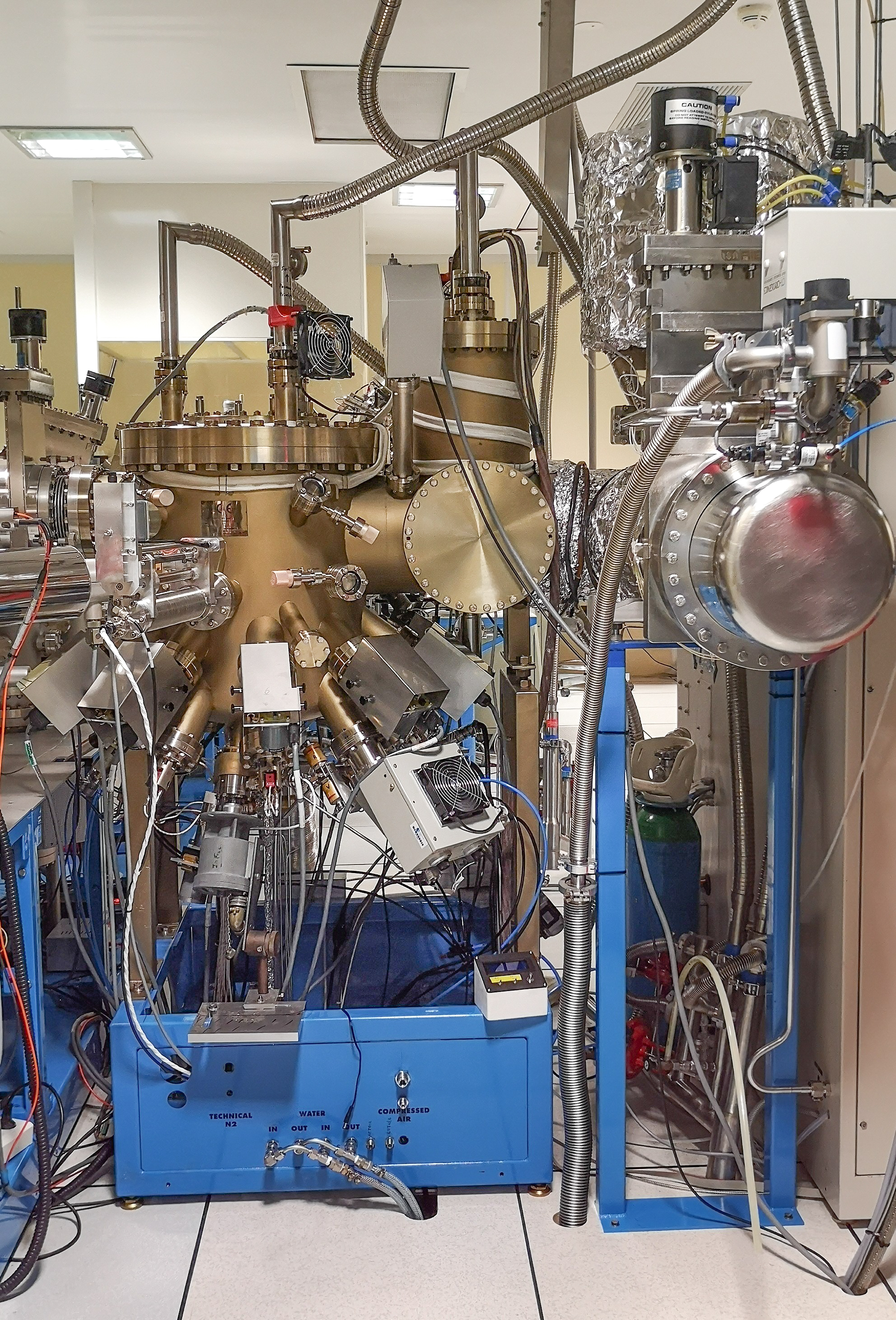
III-V MBE Riber compact 21 reactor, pump side
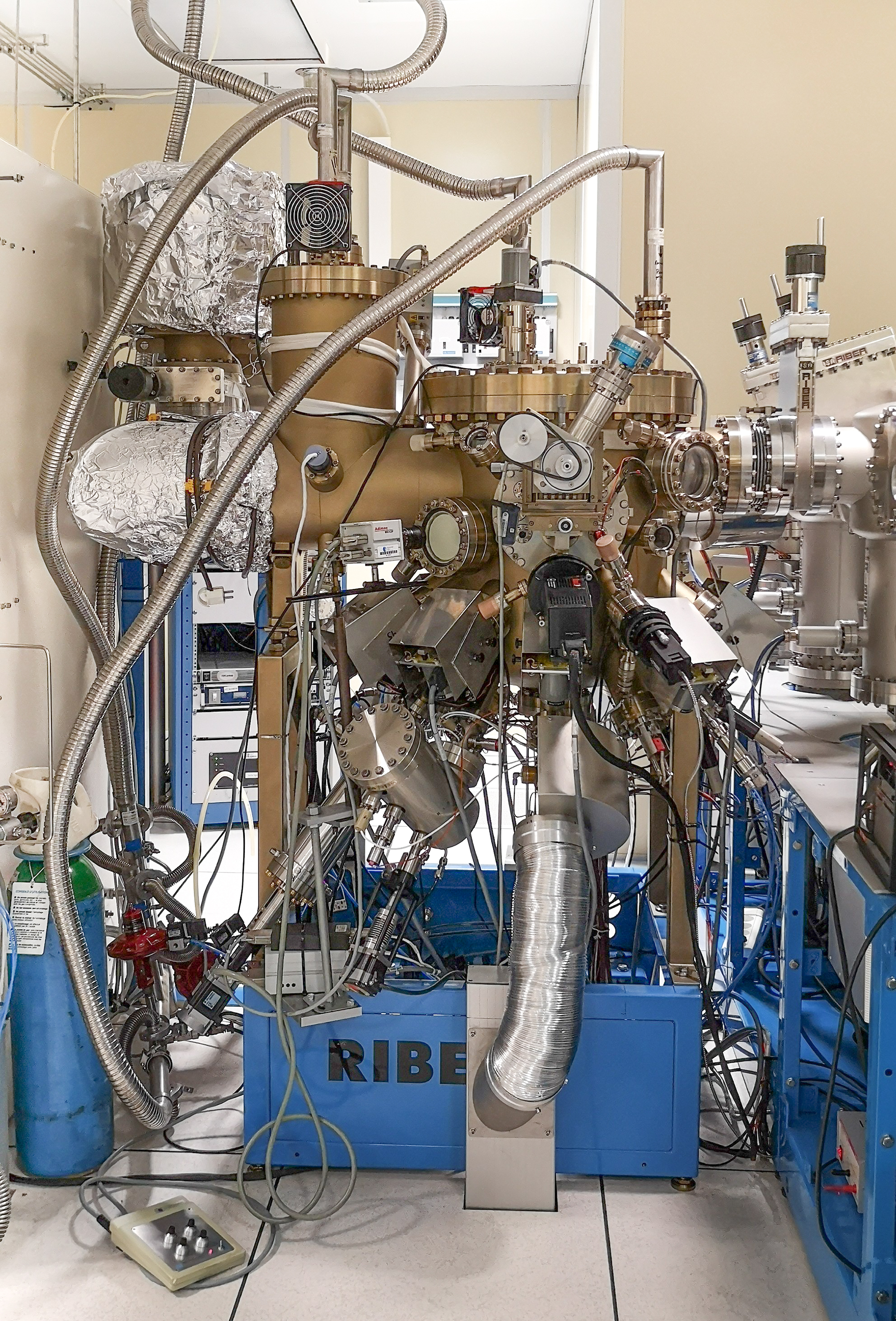
III-V MBE Riber compact 21 reactor, view from the manipulator side
Graphene/hBN epitaxy
The graphene epitaxy chamber is dedicated to the growth of the 2D materials graphene and hBN under ultra high vacuum (UHV). It is scheduled to study the elaboration of heterostructures made of these two materials. It is based on a modified RIBER COMPACT 21 chamber, fitted with the following equipments:
- a 3 in. rotatable substrate holder
- a 2 in. graphite heater which allow growth up to temperatures of 1800 K
- a carbon high temperature cell with a graphite filament (MBE-Komponenten)
- a low-flux silicon effusion cell (Riber)
- a high-flux silicon filament cell (MBE-Komponenten)
- a RF plasma nitrogen source (Riber)
- a high temperature effusion cell for boron (MBE-Komponenten)
- a high temperature gas injector for borazine B3N3H6 (Riber)
- a quadrupole mass spectrometer (Hiden Halo 201 RC) with electron energy control
- a reflected high-energy electron diffraction (RHEED) system from Staib (15S)
- temperature measurement by AOIP optical pyrometer
- flux measurements by retractable Inficon quartz balance
An UHV analysis chamber is connected to the growth chamber. It includes a Spectaleed LEED/Auger system from Omicron.

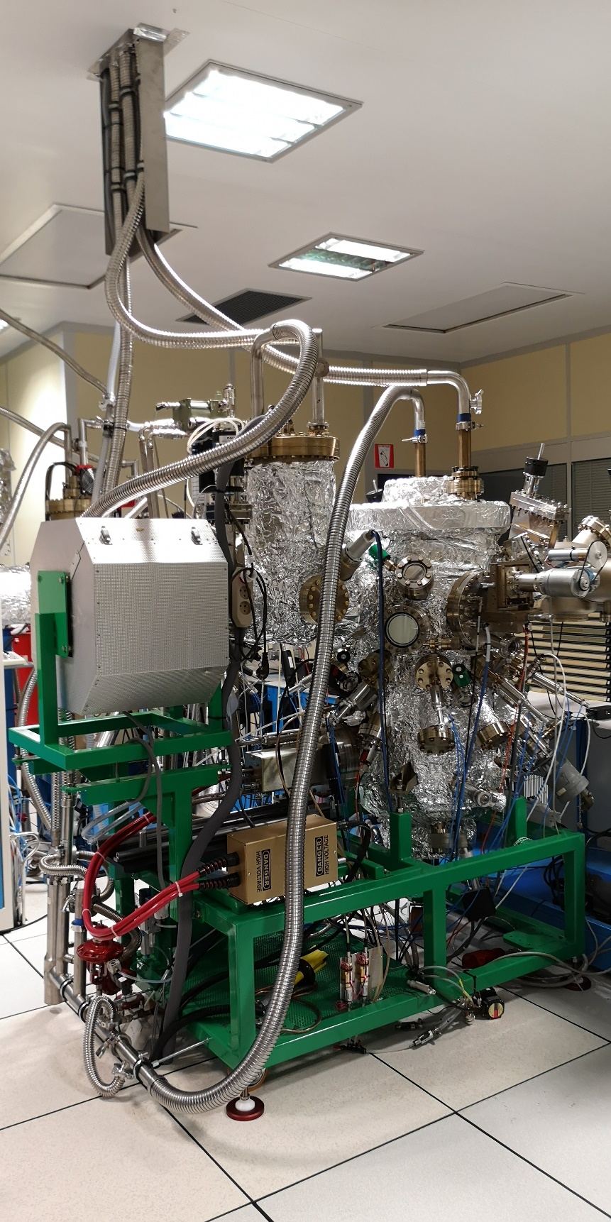
The Riber Compact 21 MBE chamber dedicated to graphene/hBN epitaxy, an overview.

The Riber Compact 21 MBE chamber dedicated to graphene/hBN epitaxy, detailed view of the growth chamber.
Graphene CVD
A chemical vapor deposition system is available, to study the catalysed growth of graphene on metallic substrates (films or foils of Cu, Ni...). It is based on a rapid thermal annealing setup JetFirst made by Jipelec, which includes the following parts:
- dry & turbomolecular pumping
- butterfly valve pressure regulation
- source gases CH4, H2 & Ar
- temperature measurement by optical pyrometry or thermocouples

Jetfirst setup: whole system
Graphene growth by CVD
The following figure shows as example the optimisation of the growth parameters to reduce the coverage by graphene bi- or multi-layers on Cu foils. This study was carried out during the GRACY ANR project ("Graphene for circuits and systems", coordinated by H. Happy, IEMN).
. Monolayer (respectively bilayer) areas are shown by white (red) arrows, from Deokar et al. Carbon 89, 82 (2015).")
Optimisation of the graphene CVD process on Cu foils (inset scale bars are 2 µm). Monolayer (respectively bilayer) areas are shown by white (red) arrows, from Deokar et al. Carbon 89, 82 (2015).
Transition metal dichalcogenide epitaxy
TMDC MBE Vinci Technologies reactor
A VINCI Technologies system, dedicated to the growth of transition metal dichalcogenides (TMDC) (Se-based), is equipped with the following sources:
- metal sources evaporated by an UHV electron gun: Tantalum, Tungsten, Molybdenum, hafnium, Niobium, Zirconium
- a Selenium effusion cell
- a Selenium valve cracker cell
- Gallium and Indium effusion cells
The system is cooled down with liquid nitrogen using a Vacuum Barrier set-up. Pumping is carried out thanks to a CTI CT8 cryo-pump and a 400l/s ion-pump.
In situ analysis can be performed thanks to the following tools:
- A RHEED Staib 15kV
- a KSA system for RHEED image acquisition and treatment.
- a Hiden HALO 201 LC system for residual gas analysis
- an optical pyrometer together with a KSA BandiT optical absorption spectrum analysis for wafer temperature measurement.
This system is coupled under ultra-high vacuum to an XPS analysis chamber and to a III-V MBE reactor.
Characterisation
X-ray diffraction

Figure 1: X-ray diffraction setup
Equipment
The X'Pert Pro diffractometer is a triple X-ray diffraction system. The X-ray beam produced by a Cu source is filtered by a hybrid 4-bounce monochromator working either in line or point focus, to filter the Kα1 (1.54 Å) line at low divergence (δθ=12″ with Ge 220 configuration). The diffracted beam can be recorded either in double-crystal configuration or using a three-bounce monochromator (3rd axis) before detection by a proportional detector. A dedicated sample holder allows grazing incidence diffraction experiments. This system is PC controlled and experimental results can be compared with simulations using the EPITAXY™ software. It is used for non-destructive control of samples, with diameter up to 100 mm.
Experiments
The applications are strongly linked to III-V semiconductor epitaxy for:
- alloy layer composition and thickness
- epitaxial layers lattice matching to the substrate
- superlattice interface quality
- thin layer strain determination
- relaxation rate and tilt of thick mismatched layers
Example: analysis of thin epitaxial Sb-based layers grown on GaAs substrate
Thanks to the high electron mobility of InAs and InSb, their small band gaps and their strong spin-orbit coupling, '6.1 Å' materials are very appealing for a number of applications in high-frequency microelectronics, mid-infrared optoelectronics and quantum technology. However, these materials suffer from the lack of lattice-matched, semi-insulating substrate, and metamorphic growth on GaAs or InP is often used for practical applications. In this case, numerous studies show strain relaxation of Sb-based III-V semiconductors grown on GaAs occurs via the formation of a Lomer dislocation array at the substrate /epilayer interface leading to a nearly fully relaxed layer. Nevertheless the threading dislocation density in the top layers remains rather high, strongly depending on the initial stages of the relaxation process. That is why we have investigated the relaxation of thin Sb-based layers and characterized their in-plane relaxation by grazing-incidence X-ray diffraction. On the spectra in figure 2, the angular spacing between the (220) reflexion of the GaAs substrate and that of the epilayer gives access to the in-plane lattice relaxation.

Figure 2: Grazing incidence X-ray diffraction spectra recorded after the growth of 16 AlSb or AlInSb monolayers on GaAs.
Micro-Photoluminescence & Raman
The micro-photoluminescence set-up is built around a LabRAM HR confocal system from Horiba Jobin-Yvon. It allows micro-luminescence measurements on low to large band gap materials, from low to
room temperature It is also used for Raman spectroscopy. Here are the main characteristics :
- 0.473 µm laser source
- f=800 mm monochromator
- CCD camera detection (0.3-1.06 µm)
- InGaAs single-channel detectors, cooled or not (0.9 to 2.2 µm)
- liquid nitrogen cooled InSb single-channel detector (1 to 5.5 µm)
- closed-cycle cryostat for microscopy Cryo Ind. (12 to 300 K)
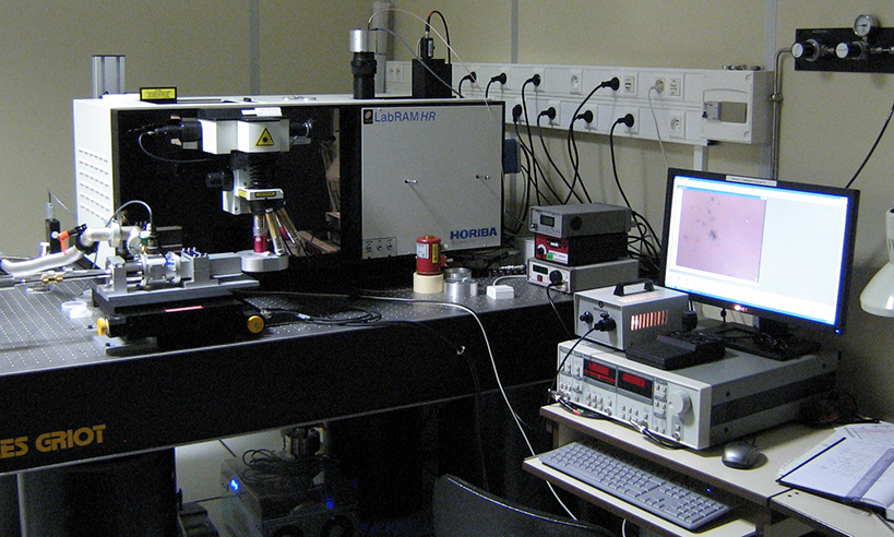
The micro-photoluminescence set-up (where the cryostat is seen front left, on its micro-positionning table).

Close-view of the microscope cryostat and coupling with the LabRAM HR.
, and Raman spectra of the circled area (bottom) (from Deokar et al., Carbon (2015) 89, 82).")
Example of Raman measurements: integrated intensity ratio map of CVD graphene after transfer on SiO2/Si (top), and Raman spectra of the circled area (bottom) (from Deokar et al., Carbon (2015) 89, 82).
Hall effect

Detail of the six probe assembly.
The HL 5500 PC system allows Hall effect measurements at room temperature, at liquid nitrogen temperature (77K) or by heating up to 600°C under controlled atmosphere. Six probes are used to contact the van der Pauw geometry or Hall bar samples so as to determine the sheet resistance of the layers. The sheet carrier density and their mobility are measured by Hall effect with a 0.32 Tesla permanent magnetic field.
Main applications:
- calibration of doping, n type and p type
- residual doping determination
- properties of two dimensional electron gas in HEMT structures
– …

The Hall effect set-up.
Electron Spectroscopy for Chemical Analysis (ESCA)
Equipment
The surface analysis system is connected to 2 molecular beam epitaxy chambers under ultra-high vacuum and to an introduction chamber, which allows the analysis of any sample. Based on a 5600 Physical Electronics system, the set-up has been adapted to work on 3-inch MBE sample holders. The main parts are:
- sample manipulator with 3 translations and 2 rotations (polar and azimuth)
- 150 mm radius hemispherical analyser
- X-ray dual anode Zr(2042eV)/Mg(1254 eV)
- monochromatic X-ray source Al (1487 eV)
- 8 keV electron gun with a 20 µm minimum spot size
- 5 keV ion gun
- He I (21.2 eV) and He II (40.8 eV) UV lamp
- neutralise electron gun
- Low Energy Electron Diffractometer (LEED)
- In XPS experiments, the ultimate resolution is 0.45 eV, measured as the FWHM of the Ag 3d5/2 core level line.
In XPS experiments, the ultimate resolution is 0.45 eV, measured as the FWHM of the Ag 3d5/2 core level line.

Figure 1: General views of the ESCA system
Experiments
The know-how developed around the IEMN ESCA system concerns:
- the MBE grown III-V semiconductor surfaces and interfaces
- the characterization of process steps during device fabrication
- the grafting of organic layers
Moreover, this system is available for any kind of analysis from outside the laboratory.
Example: ESCA analysis of InGaAs surface after ALD oxide deposition
IEMN has an important activity in the semiconductor processing for the fabrication of opto and micro-electronic devices. In this context, XPS is used to characterize various processing steps, such as etching, annealing.......For instance, one such study has concerned the characterization of the ALD oxide deposition on InGaAs for the fabrication of III-V MOS structures by the IEMN "Anode" group. Figure 2 shows the As3d and Ga3d/In4d XPS core level lines recorded in non-optimized conditions, showing important InGaAs oxidation. On the contrary, in optimized conditions (figure 3), the XPS spectra do not reveal any oxide components on the InGaAs surface.
 and Ga3d/In4d (right) XPS spectra recorded after ALD oxide deposition on InGaAs in non-optimized conditions. The InGaAs surface is heavily oxidised.")
Figure 2: As3d (left) and Ga3d/In4d (right) XPS spectra recorded after ALD oxide deposition on InGaAs in non-optimized conditions. The InGaAs surface is heavily oxidised.
 and Ga3d/In4d (right) XPS spectra recorded after ALD oxide deposition on InGaAs in optimized conditions. Oxide related XPS peaks have disappeared.")
Figure 3: As3d (left) and Ga3d/In4d (right) XPS spectra recorded after ALD oxide deposition on InGaAs in optimized conditions. Oxide related XPS peaks have disappeared.
Thermal Analysis
Thermogravimetric Analysis coupled with Mass spectrometry (TG/MS)
TG/MS Analysis is used to study the thermal behavior of any material (polymers, organic or inorganic, liquid or solid, film, fibers, powder, monolith) while exposed to heating and gas environment. Samples can be treated under various atmospheres.

Figure 1: Thermogravimetry coupled with mass spectrometry apparatus
Gas environment available:
Inert atmosphere(He, N2Ar,)
Oxidizing atmosphere(2% O2 in He, 20%O2 in He)
Reducing atmospherediluted hydrogen (3% H2 in Argon), and NH3
Humid atmosphereInert and oxidizing atmospheres
Instrumentation includes 2 different systems:
- NETZSCH STA 449 F1- covers a temperature ranging from 25 to 1500°C
- NETZSCH STA 409- covers a temperature ranging up to 2000°C.
The two TGA systems are coupled with Quadrupole mass spectrometry (QMS) analysis. Line (capillary-type interface) connecting the TGA to MS can be heated to 300°C.

Figure 2: TG/MS: Thermal decomposition of hybrid organic-inorganic polymer in helium at 10°C/min
Specifications
Sample required
5-30 mg is the minimum mass required for sample analysis.
Samples should be non-explosive and non-corrosive.
 Brand: Setaram-France")
Figure 3: Differential calorimeter (up to 600°C) Brand: Setaram-France
Differential Scanning Calorimetry (DSC)
DSC provides a convenient method of measuring heat capacities and enthalpy changes. Commercial instruments provide a recorder output of the constant-pressure heat capacity,(Cp) as a function of temperature.
DSC method can be used for the analysis of energetic effects such as:
- Melting / crystallization behaviour
- Solid-solid transitions
- Polymorphism
- Glass transitions
- Cross-linking reactions
- heat capacity measurements
Contact details
Dr D. Hourlier
Institute of Electronics, Microelectronics and Nanotechnology
IEMN UMR 8520, Avenue Henri Poincare, BP 60069 F-59652 Villeneuve d'Ascq Cedex-France
Room 133/135
Contact : djamila.hourlieruniv-lille.fr


