
MICROELEC Silicon Group
WELCOME TO THE SILICON MICROELECTRONICS GROUP AT IEMN
The group brings together researchers, staff and students working in the following two areas:
i) Design of integrated circuits for communication systems and artificial intelligence
ii) Functional packaging and integrated micro-thermics
Design of integrated circuits for communication systems and artificial intelligence
On the one hand, we design and demonstrate new high-performance, low-power, highly integrated communication systems based on CMOS technologies. This involves designing circuits and systems for a wide range of frequency bands (RF to mmW), as well as for various communication standards, such as Bluetooth, Wi-Fi, cellular and satellite, or non-standardised protocols. This is illustrated by our work on high-speed, low-power capacitive communications coupled to the human body (see portfolio). We are also developing integrated ultra-low-power architectures to provide hardware solutions for artificial intelligence at the extreme edge. We are focusing on demonstrating new breakthrough concepts such as event-driven signal processing, in-memory computing, hardware implementation of ultra-low-power machine learning algorithms and neuromorphic processors with non-volatile memories. The applications envisaged include the processing of audio signals (recognition of key words and sounds), biomedical signals (detection of cardiac arrhythmia or sleep apnoea) or movement (detection of falls or fine movements). The concepts developed are based on advanced industrial CMOS technologies (28nm and 18nm FDSOI CMOS).
Digital transmitter architecture for RF applications
![]()
Body-coupled communications

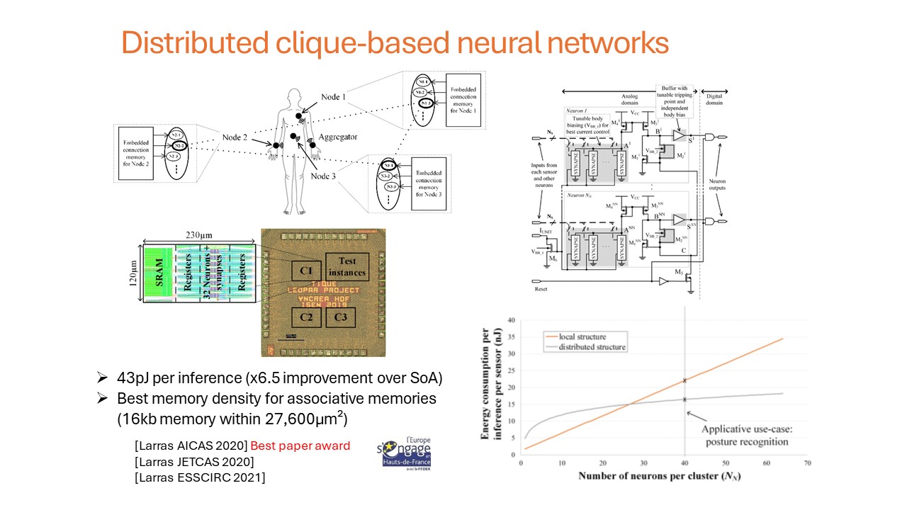
On-chip neural networks for near-sensor computing / Edge AI
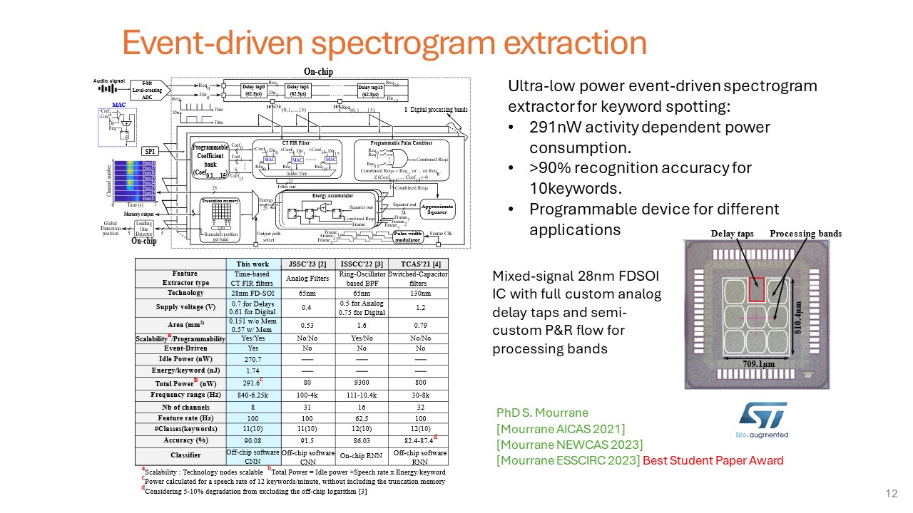
Event-driven signal processing for in-sensor feature extraction
Functional packaging and integrated micro-thermics
For 10 years now, the group has been focusing on two complementary areas to meet the challenges of microelectronics: i) functional packaging, which responds to the increasing complexity of heterogeneous assemblies, particularly in the RF and mmW fields ii) studying the limitations and opportunities associated with managing heat flows in circuits and systems.
Functional packaging aims to develop advanced heterogeneous integration solutions in line with the 'System Moore' paradigm, according to which significant performance and compactness margins can be gained by assembling sub-systems. For example, by integrating mmW and optical waveguides on an interposer, functional packaging enables mmW chips and photonic chips to be embedded and connected on the same heterogeneous assembly platform for the synthesis of electro-optical transceivers. This activity also covers the implementation of chips in the D, G and J band spectrum (110 to 320 GHz), which requires the development of complex packages in order to limit losses linked to propagation and mode transitions. This area of research relies in particular on the use of laser micromachining techniques (EQUIPEX LEAF) to address dimensions ranging from the micron to the millimetre, compatible with the dimensions of waveguides in the bands concerned. (see portfolio noise source)
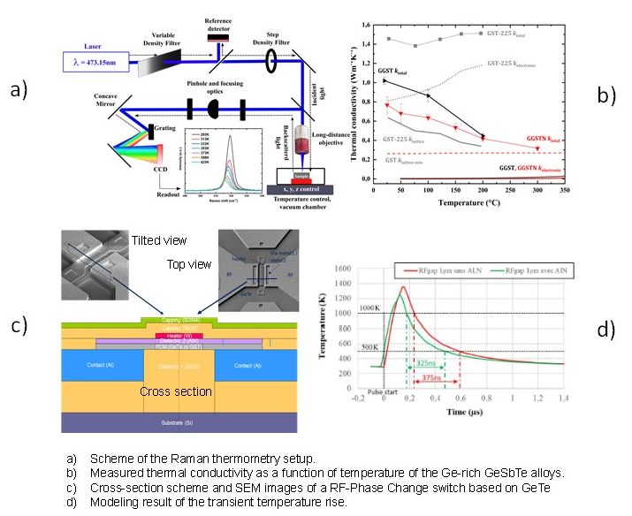
Heat transfer limits the performance of the most integrated technologies. This problem is exacerbated by the highly heterogeneous and truly nanometric assemblies of materials in components. On the other hand, heat has become an operational resource for certain components (phase-change memories, thermo-optic modulation, RF switches). Our aim is to contribute to the modelling, manufacture and thermal and electrical characterisation of materials and components. In addition to Raman thermometry, near-field thermal microscopy and the 3Ω method, the instrumentation project currently under development is based on the acquisition of a time-resolved (50 ns), multi-wavelength thermo-reflectance bench capable of measuring temperature transients on a wide variety of microelectronic systems.
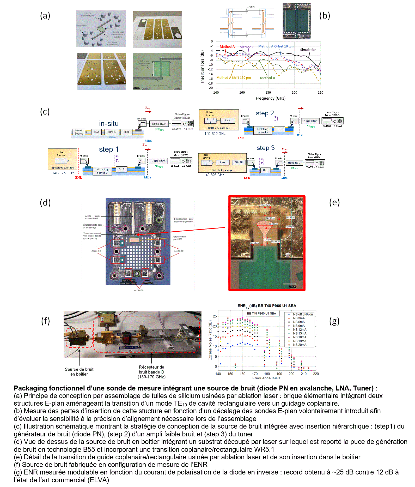
Packaging of integrated active millimetre-band probes
Advanced silicon technologies (BiCMOS B55 STMicroelectronics) targeting cut-off frequencies fT/fmax above 400GHz will enable the design of silicon circuits in the 140-220GHz frequency range (G-band). In order to validate the development of these technologies, microwave characterisation resources are needed to extract transistor merit factors such as noise figure and power efficiency, and to develop the associated modelling. At these frequencies, broadband tools such as noise sources, noise receivers, impedance adapters (tuners) and power receivers are not currently available on the market to meet this demand. Previous thesis work has demonstrated the possibility of implementing these functions by embedding them directly on silicon around the device to be tested in BiCMOS B55 technology. This test approach in-situ or built-in self test (BIST) is not, however, a viable solution because it consumes a substantial amount of silicon, resulting in an unacceptable cost.
In order to take advantage of measurement instrumentation for a range of technologies beyond just the B55 process, and to rationalise the costs associated with testing, the next step is to design the integration of these functions into a compact system positioned as close as possible to the measurement peaks. The proximity of the instrumentation function (e.g. noise source) to the immediate vicinity of the tip is made necessary in order to control losses, variations in which drastically alter the measurement sensitivity (MDS - minimum detectable signal) and the impedance constellation at the input of the component to be measured.
This measurement system must be produced using a packaging technology that integrates the manufacture of the tips in order to test the components directly on the silicon wafers. This instrumentation system therefore takes the form of a functionalized active probe requiring the implementation of a waveguide technology similar to that described in the previous section. This research theme has given rise to initial developments, illustrated below, explaining the manufacture and measurement of elementary technological building blocks, as well as the implementation strategy for this type of probe.
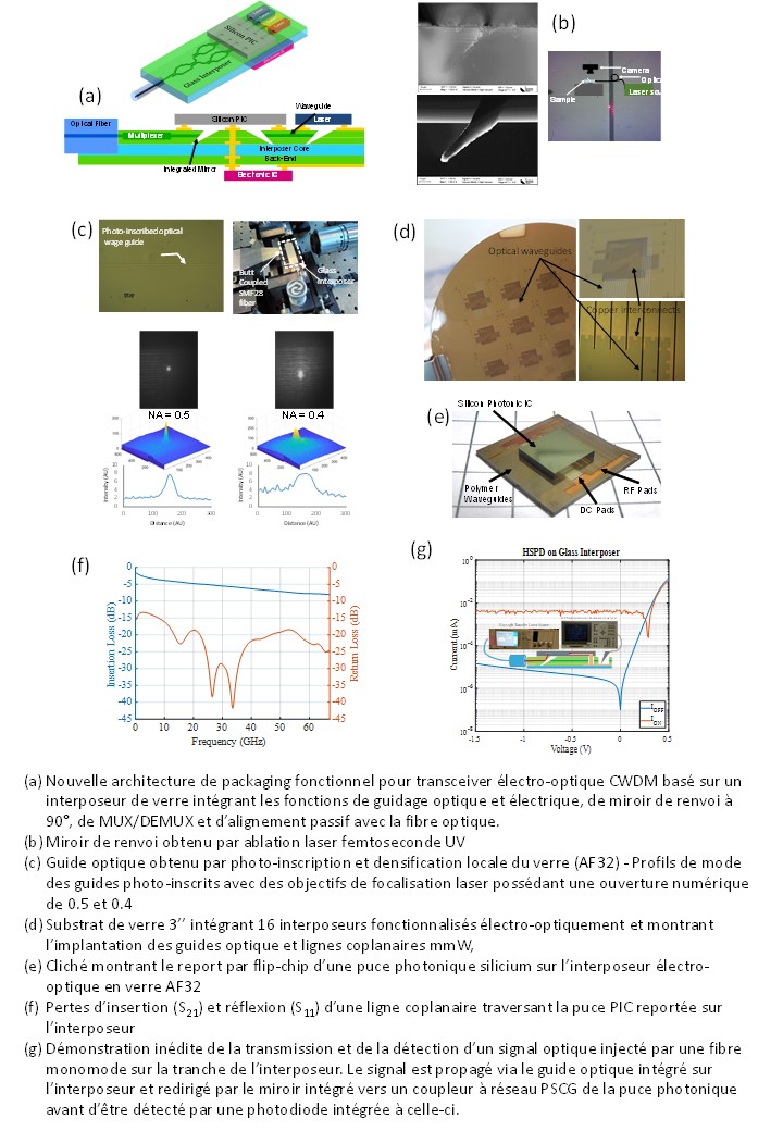
Electro-optical interposer for 400Gb/s high-speed communication
This project involved the study and development of an interposer incorporating electrical and optical functions integrated into a glass substrate, with the aim of validating a complete passive CWDM transceiver assembly based on STMicroelectronics' PIC25G silicon photonics technology. Firstly, this work addressed the design and fabrication of the main elementary functions integrated into the interposer, namely, single-mode waveguides, vertical optical coupling structures and transmission lines operating at mmW RF frequencies. Secondly, the functionality of the interposer and the complete assembly was demonstrated through detailed electrical, optical and mixed-mode characterisation work. In terms of metrics, we fabricated an interposer incorporating waveguides with propagation losses of < 6 dB/cm at 1310 nm, 1 cm coplanar transmission lines with insertion losses of 3 dB at 60 GHz, optical signal redirection mirrors and all the electrical and optical routing needed to test the detection and modulation of light by the PIC25G silicon photonic chip. The PIC25G chip was assembled on the interposer using a conventional flip-chip technique with no active alignment. This work demonstrated the viability of the glass interposer approach for silicon photonic packaging using conventional assembly techniques in the microelectronics industry. This work is part of the EQUIPEX LEAF project, the ST-IEMN joint laboratory and the NANO2022 research programme.
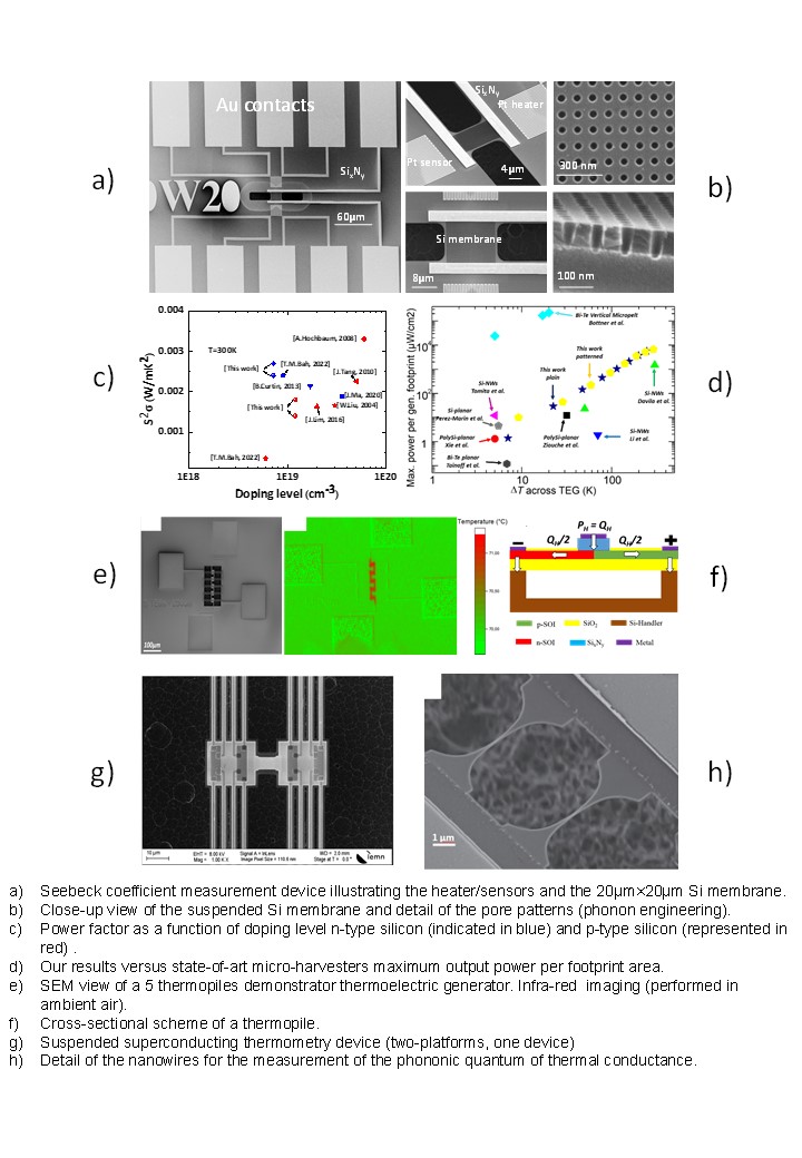
Suspended crystalline silicon micro-platforms for thermal and thermoelectric characterisation
Size reduction in nanosctructures has a strong impact on thermal conductivity via reducing the mean free path of phonons. This effect can be exploited to artificially enhance the thermoelectric properties of materials. This idea was deployed as part of the UPTEG ERC and via three CIFRES theses as part of the STMicroelectronics-IEMN joint laboratory. We have developed suspension processes for crystalline silicon structures (membranes, phononic structures, nanowires) equipped with thermoresistive elements. The thermal and thermoelectric metrology of such objects remains a challenge. We were thus able to quantify the reduction in thermal conductivity and produce a demonstrator of an integrated thermoelectric converter. More recently, as part of Hafsa Ikzibane's thesis, we were able to quantify the thermoelectric properties of ultra-thin membranes (60 nm) and the impact of a nano-porous structure. Finally, these processes are currently being used as part of the ANR HANIBAL project to design superconducting thermal sensors to study heat transfer in the quantum regime.

Modelling and thermal metrology for phase-change components
Heat transfer limits the performance of the most integrated technologies. This problem is exacerbated by the highly heterogeneous and truly nanometric assemblies of materials in components. On the other hand, heat has become an operational resource for certain components (phase-change memories, thermo-optic modulation, RF switches). Our aim is to contribute to the modelling, manufacture and thermal and electrical characterisation of materials and components. To do this, we use Raman thermometry, near-field thermal microscopy and the 3ω method. The instrumentation project currently under development is based on the acquisition of a time-resolved (50 ns), multi-wavelength thermo-reflectance bench capable of measuring temperature transients on a wide variety of microelectronic systems. Two representative examples of this activity are: i) the Raman thermometry study of germanium-enriched GeSbTe, a phase-change material at the heart of memory technologies. (Cifre thesis STMicroelectronics - Akash Patil). ii) Thermal modelling of RF switches for 5G using a GeTe RF channel (Cifre thesis STmicroelectronics - CEA Leti -IEMN by Corentin Mercier).