


 The Lille branch of the CNFM
Director: Virginie Hoël virginie.hoel![]() univ-lille.fr
univ-lille.fr
Since 1982, the cluster has forged its expertise in the design, manufacture and characterization of components in the RF and HF domains and in 2017, the project was extended to RFID with in 2018 a deployment in Microscopy Near Field Microwave.
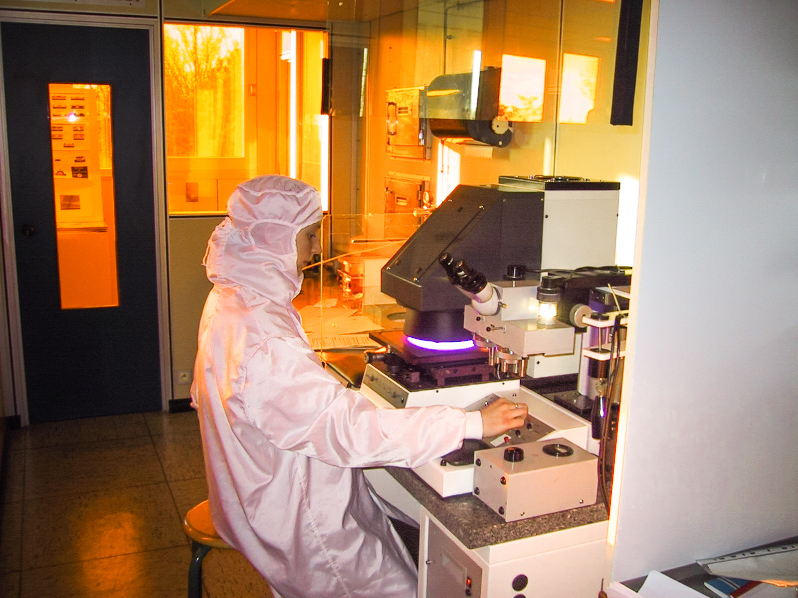
Located on the campus, in the historical building of the IEMN, the CNFM-Lille has a 300 m2 clean room with training facilities for students, academics and professionals in microelectronics. It is open to the public and to secondary schools during the Fête de la science.
Lille students projects at the CNFM: a real gateway to the microwave engineering professions
The students of the Master Networks and Telecommunications course Syscom (Communicating Systems) of the University of Lille presented their final work in the amphitheater of the IEMN. Just like their dynamic presentation, they worked in a very interactive way, thinking together about the problems they faced. They developed two projects that aim to develop microwave solutions for the Smart City in the field of "CAD, realization and validation of passive and active microwave functions":
- a 1-port vector network analyzer at 2.45 GHz for non-destructive testing (NDT), in space, nuclear and other applications. Advantages: low cost and minimal space requirements, easy integration and passive power consumption.
- a 6.2 GHz monostatic scalar bio-radar for simultaneous measurement of objects wearables. Challenges: compactness, ubiquity, low cost.
Carefully supervised by their teachers Gilles Dambrine, Virginie Hoël and Kamel Haddadi, as well as the technical manager of the center for the circuit assembly part, the work was carried out in three stages:
- technological manufacturing for the planar structure
- design on CAD tools provided by CNFM National Services
- tests and validations
Details of the projects and funding of the Lille cluster
|
Year FINMINA |
Project title |
Amount of the project |
Support FINMINA |
Cofinancement |
|
2012-2013 |
Characterization and test equipment: vector network analyzer |
40 k€ |
20k€ |
20 k€ |
|
2012-2013 |
Development of components on flexible substrates for RF applications |
30 k€ |
15 k€ |
|
|
2014-2015 |
Graphene - Fabrication and structural characterization |
100 k€ |
30 k€ |
70 k€ |
|
2016-2017 |
Characterization of 2D materials by Raman spectro |
60 k€ |
20 k€ |
40 k€ |
|
2017-2018 |
Object location by RFID technique |
20 k€ |
10 k€ |
10 k€ |
|
2018-2019 |
Microwave near field microscopy |
11 k€ |
5 k€ |
6 k€ |
|
End of 2019 |
Characterization of an IoT RF system in its operating environment |
30 k€ |
7 k€ |
23 k€ |
 The GIP-CNFM: a national network
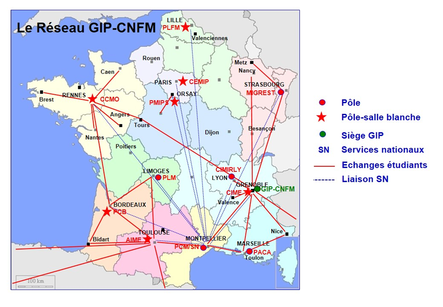
The National Coordination for Training in Microelectronics and Nanotechnology (CNFM) is a Public Interest Group (GIP) dedicated to training and innovation in higher education. The CNFM group, made up of academics and industrialists, meets regularly under the aegis of the professional association ACSIEL Alliance électronique.
The 12 national clusters groups together technological means for manufacturing, Computer Aided Design (CAD) and characterization in Micro and Nanoelectronics in inter-university or inter-regional centers, some of which are equipped with clean rooms, in line with research and industrial partners. These centers welcome students and teachers from many schools and universities on dedicated platforms.
The network's activities
- The Pedagogical Days (JPCNFM) held on one of the poles take place every two years. They aim to encourage exchanges of a pedagogical nature between teachers and, for professionals, to follow the adaptation to new technologies (Program of the Fifteenth Pedagogical Days).
- The Journées Nationales du Réseau Doctoral en Micro-nanoélectronique (JNRDM) are renewed every year and allow young researchers to present their work (Program of the 21st edition).
- The network also publishes a newspaper The Flea in Your Ear devoted to the life of the network.
The GIP-CNFM, winner of the IDEFI with the FINMINA project
As part of the PIA (Plan des Investissements d'avenir) and since 2012, the GIP-CNFM has benefited from the FINMINA program (National Network for Innovative Training in Micro- and Nanoelectronics). The financial support, which amounts to 4.4€ over eight years, contributes to the implementation of a long-term modular training program adapted to students, technicians and engineers throughout their lives. In addition, the project has received the IDEFI label (Initiative d'Excellence en Formations Innovantes), which reinforces the prestige and international attractiveness of French training in the field of nanotechnology.
The IDEFI-FINMINA program thus targets a number of actions among which the strengthening of partnerships between academia and industry, the opening towards continuing education and the enhancement of a base of know-how in international cooperation.
Thanks to the FINMINA program, 90 innovative projects have emerged since its inception in 2012 in many fields covering advanced research: DAC, embedded electronics, advanced technologies (silicon, organic, thin films, optoelectronics, 2D components), sensors and actuators (physical, mechanical, optical, chemical, biological), communication systems and connected objects. See the GIP-CNFM Orientation Council 2018.


