


Epitaxial growth
Chemical Vapour Deposition (CVD)
Physical Vapour Deposition (PVD)
Inkjet printing
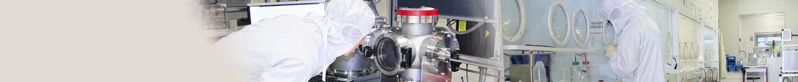
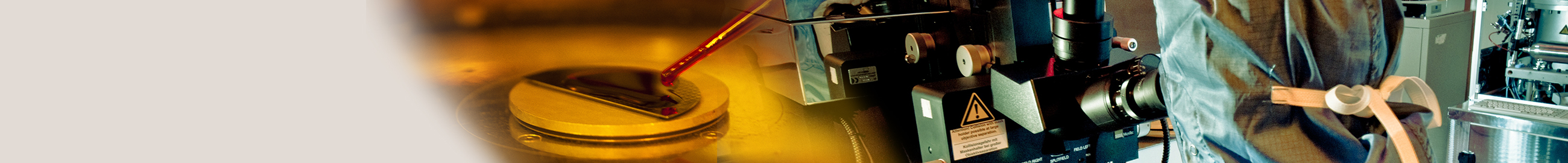
The micro-nanofabrication facility offers a wide range of thin-film deposition techniques to cover a wide variety of material properties. For several years, we have capitalized on our know-how in many fields such as :

- deposits of materials for energy storage in atomic or thin conformal layers
- the silicium technology for microelectronics and MEMS/NEMS
- multilayers of magnetic and multi-ferroic nanostructured materials
_ organic deposits for biosystems, organic and molecular electronics
- metal deposits used for contact the active layers components of several dies (Si, III/V, III/N)
- growth and integration of monolayer or multilayer graphene in components
- deposits located by inkjet printing for flexible microelectronics
These activities are based on a range of techniques grouped into major areas: chemical vapour deposition, physical vapour deposition, chemical synthesis and surface functionalisation, inkjet printing, heat treatment and epitaxy.
Contact Depot manager - Isabelle ROCH-JEUNE
isabelle.roch-jeune![]() iemn.fr
iemn.fr
Contact Epitaxy manager - Christophe COINON
christophe.coinon![]() iemn.fr
iemn.fr


