IEMN
  • Home
  • News
    • IEMN Newsletters
    • M2-Ingé Internships
    • Job offers
    • All news
  • The Institute
    • Presentation
    • Organization of the institute
    • The Scientific Department
    • The Technological Department
    • Administrative and financial management
    • Rules of procedure
    • Our commitments
  • The Research
    • Scientific departments
      • Nanostructured Materials and Components
      • Micro / nano optoelectronics
      • Telecommunications Technologies and Intelligent Systems
      • Acoustic
    • Research groups
    • Flagship
  • Scientific Production
    • IEMN publications
    • Scientific production resources
  • The platforms
    • CMNF - Central Platform for Micro Nano Manufacturing
      • Engraving and implantation pole
      • In Line Analysis Unit
      • Soft Lithography and Bio Microfluidics
      • Deposits and epitaxy division
      • Lithography Unit
      • Packaging Division
      • CMNF Staff
    • PCMP - Multi-Physics Characterization Platform
      • Scanning Probe Microscopy Facility
      • Hyperfrequency, Optical and Photonic Characterization (CHOP)
      • Advanced Communications Systems and Prototyping cluster (SigmaCOM)
      • Characterisation, ElectroMagnetic Compatibility and Prototyping Centre (C2EM)
      • PCMP Staff
    • Services offered by our platforms
  • Partnership - Valuation
    • Academic Collaborations
    • ANR Projects
    • Main international collaborations
    • Industrial partnerships
    • The joint IEMN-Industry laboratories
    • Startups
  • Research Training
    • After the thesis
      • Do a post-doc at the IEMN
      • Towards the world of business and industry
      • Become a teacher-researcher
      • Become a Researcher
      • Starting a business at IEMN
      • FOCUS on a SATT engineer from the IEMN
    • A thesis at IEMN
      • Thesis and HDR defenses
      • Thesis topics
      • Financing
      • Doctoral studies
    • Master - Engineer
      • Masters ULille
        • Master Life Sciences and Technologies graduate programme
        • Master Nanosciences and Nanotechnologies - Speciality ETECH
        • Master Networks and Telecommunications
      • UPHF-INSA Masters
        • Master in Embedded Systems and Mobile Communications Engineering
        • Master Cyber Defense and Information Security
        • Master in Materials, Control and Safety
        • Master in Image and Sound Systems Engineering
      • Partner/Tutoring Engineering Schools
      • M2-Ingé Internships
    • The Lille branch of the GIP-CNFM
    • Nano-École Lille
  • Contact Us
    • Location
    • Contact form
    • Annuaire Intranet
  • Our support
  • fr_FR
  • Rechercher
  • Menu Menu
PCP : PÔLE CHAMP PROCHE
Slide thumbnailPCP : PÔLE CHAMP PROCHE

UHV domain

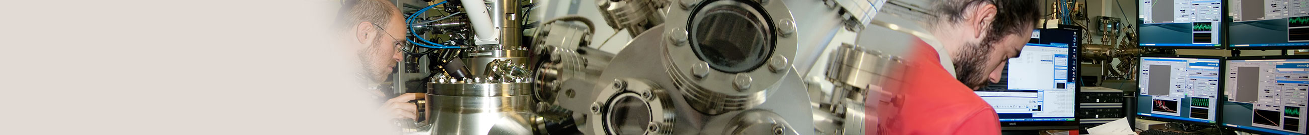
Les 5 instruments Ultra-vide (UHV) de l’IEMN couvrent une large gamme de caractéristiques permettant de répondre aux demandes les plus pointues des scientifiques dans les domaines des nanosciences, de l’électronique ou des technologies de rupture.

Capables d’imager et d’analyser les propriétés de toute surface à l’the atomic scale., ces microscopes sont installés dans des bâtis UHV dotés de moyens de préparation et d’analyse annexes. Ces dispositifs permettent de mener une étude complète in-situ, de l’élaboration à la caractérisation d’un matériau.

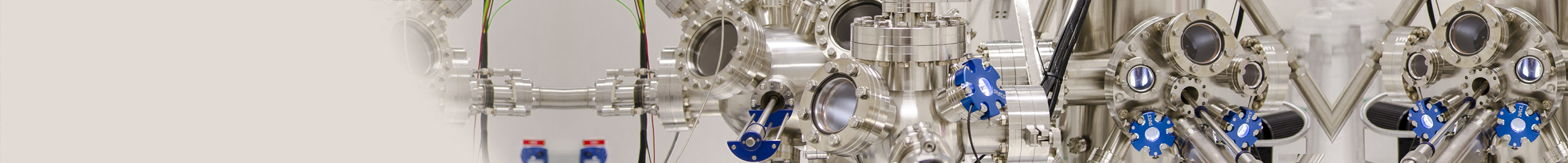
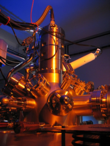
Exemples d’équipements : Omicron RT-STM, VT-AFM/STM, LT-STM, Nanoprobe. SPECS JT-AFM/STM. Laser Ti:Sapphire Spectra-Physics Mai-Tai HP.

Deposits of organic thin films under vacuum are also proposed (parylene, pentacene,...).

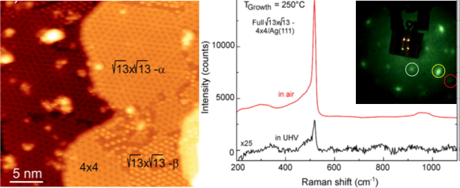
  • Croissance d’une monocouche de silicene sur Ag(111) et étude combinée STM, STS (T=77K), LEED et Raman.

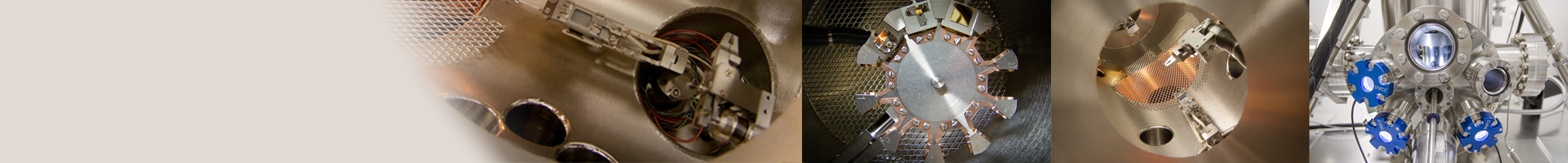
    Préparation in-situ d’échantillons, dépôt et croissance de nanostructures, analyse combinée de surfaces par spectroscopie AUGER, diffraction d’électrons lents (LEED) et STM

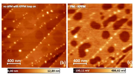
  • Mesure des transferts de charge entre nanocristaux dopés et leur environnement par KPFM

    Analyse topographique et spectroscopique sur tous types de matériaux, à l’échelle atomique, sur une large gamme de températures (1 à 500K), sous champ magnétique (3 Teslas) par microscopie AFM, STM, EFM, KPFM

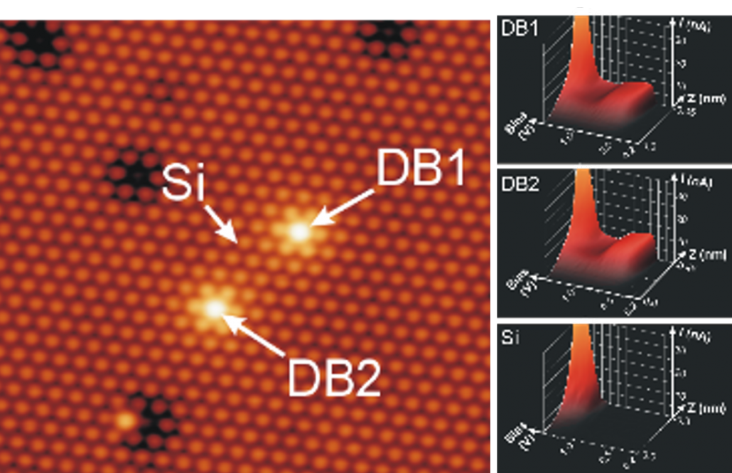
  • Mesure STM et STS (T=4K) du coefficient de capture d’un état quantique isolé (liaison pendante sur une reconstruction de la surface (111) de silicium dopé bore)

    Nanomanipulation, transport électronique multi-échelles, analyse couplée MEB/STM multipointes sur des systèmes complexes (hétérostructures, composants) et matériaux de faible dimensionnalité individuels (matériaux 1D : nanofils, nano-poutres, nano-ressorts ; matériaux 2D : graphène, silicène, etc.)

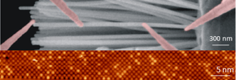
  • Étude combinée: mesure 4 pointes du transport électronique à l’échelle nm dans des nanofils InAs isolés + dépôt et imagerie STM à l’échelle atomique de nanofils InAs

    Dépôt de nanofils et de molécules organiques

Autres expertises

  • Cryo-magnéto-transport (9 Tesla, 1.7K)
  • Développement instrumental, couplage de techniques : AFM/MEB, Laser femto-seconde/STM/MEB, Raman/STM en UHV
  • Croissance de matériaux 2D et de nanostructures sur demande
  • Analyse chimique des surfaces par Auger et LEED
  • Raman sous ultra Vide

Contact:

Maxime BERTHE (STM, STS, Nanoprobe/4 pointes)
maxime.bertheiemn.fr 03 20 19 79 79

Sylvie GODEY (STM/AFM, KPFM)
sylvie.godeyuniv-lille.fr 03 20 19 79 79

Application areas: Topography, Physical Nanocaracterization

Key words : AFM, CAFM, PFM, SthM, EFM/KPFM, Nanomechanique

  • CMNF - Micro and Nano Fabrication Center
    • CMNF Staff
    • Deposits and epitaxy division
      • Chemical Vapour Deposition (CVD)
      • Physical Vapour Deposition (PVD)
      • Inkjet printing
      • Heat tratments
      • Chemical synthesis and surface functionalisation
      • Epitaxial growth
    • Lithography Unit
      • Electronic Lithography
      • Optic Lithography
      • 2D laser lithography
      • Collage
    • Engraving and implantation pole
      • Etching and plasma treatment
      • Deep etching of silicon
      • Chemical vapor etching
      • Ion beam etching
      • Focused Ion Beam
      • Ion implantation
      • Wet etching and surface preparation
    • In Line Analysis Unit
      • Structural characterizations
      • Electrical properties
      • Propriétés optiques et spectroscopies
      • Microscopy Topography Morphology
      • Faisceau / beam
    • Soft Lithography and Bio Microfluidics
      • Soft lithography
      • BioMicroFluidics
    • Packaging Division
      • Shaping chips and wafers
      • Component assembly
      • Precision machining
  • PCMP - Multi-Physics Characterization Platform
    • PCMP Staff
    • Scanning Probe Microscopy Facility
      • Air Domain
      • UHV domain
    • Hyperfrequency, Optical and Photonic Characterization (CHOP)
      • Spectroscopy
      • Static - Small signal - Noise
      • Power
      • Nano characterisation
      • MEMS
      • Microwave photonics
      • Millimetre and THz
      • Temperature measurements
    • Characterisation of COMmunicating Systems and Prototyping cluster (SigmaCOM)
      • Analog and digital communication systems
        • Energy efficiency test bench
        • Multifunctional analogue and digital I/O devices
        • Software-defined radio
        • Telecom test bench
      • Optical communication systems
      • Prototypage (SigmaCom – C2EM)
        • Design Modelling
        • Programming
        • Achievements
        • Tests & Measurements
    • Characterisation, ElectroMagnetic Compatibility and Prototyping Centre (C2EM)
      • Anechoic chamber
      • TEM cell
      • Reverberation chamber with mode mixing
      • MaMIMOSA
      • Measurement Zt
  • Services offered by our platforms
    • services of the Bio Micro Fluidic platform
    • Services of the CMNF platform
Logo
Cité Scientifique
Avenue Henri Poincaré
CS 60069
59 652 Villeneuve d'Ascq Cedex, France
Tel : 03 20 19 79 79
CNRS Logo University of Lille Logo University Polytech Logo Junia Logo Centrale Lille Logo Renatech Logo RFnet Logo
Site map
Copyright Service ECM et pôle SISR 2024
  • Scientific production
  • Legal information
  • Privacy policy
Faire défiler vers le haut
fr_FR
fr_FR
en_GB
We use cookies to ensure you have the best experience on our website. If you continue to use this site, we will assume that you are happy with it.OKNoPrivacy policy