IEMN
  • Home
  • News
    • IEMN Newsletters
    • M2-Ingé Internships
    • Job offers
    • All news
  • The Institute
    • Presentation
    • Organization of the institute
    • The Scientific Department
    • The Technological Department
    • Administrative and financial management
    • Rules of procedure
    • Our commitments
  • The Research
    • Scientific departments
      • Nanostructured Materials and Components
      • Micro / nano optoelectronics
      • Telecommunications Technologies and Intelligent Systems
      • Acoustic
    • Research groups
    • Flagship
  • Scientific Production
    • IEMN publications
    • Scientific production resources
  • The platforms
    • CMNF - Central Platform for Micro Nano Manufacturing
      • Engraving and implantation pole
      • In Line Analysis Unit
      • Soft Lithography and Bio Microfluidics
      • Deposits and epitaxy division
      • Lithography Unit
      • Packaging Division
      • CMNF Staff
    • PCMP - Multi-Physics Characterization Platform
      • Scanning Probe Microscopy Facility
      • Hyperfrequency, Optical and Photonic Characterization (CHOP)
      • Advanced Communications Systems and Prototyping cluster (SigmaCOM)
      • Characterisation, ElectroMagnetic Compatibility and Prototyping Centre (C2EM)
      • PCMP Staff
    • Services offered by our platforms
  • Partnership - Valuation
    • Academic Collaborations
    • ANR Projects
    • Main international collaborations
    • Industrial partnerships
    • The joint IEMN-Industry laboratories
    • Startups
  • Research Training
    • After the thesis
      • Do a post-doc at the IEMN
      • Towards the world of business and industry
      • Become a teacher-researcher
      • Become a Researcher
      • Starting a business at IEMN
      • FOCUS on a SATT engineer from the IEMN
    • A thesis at IEMN
      • Thesis and HDR defenses
      • Thesis topics
      • Financing
      • Doctoral studies
    • Master - Engineer
      • Masters ULille
        • Master Life Sciences and Technologies graduate programme
        • Master Nanosciences and Nanotechnologies - Speciality ETECH
        • Master Networks and Telecommunications
      • UPHF-INSA Masters
        • Master in Embedded Systems and Mobile Communications Engineering
        • Master Cyber Defense and Information Security
        • Master in Materials, Control and Safety
        • Master in Image and Sound Systems Engineering
      • Partner/Tutoring Engineering Schools
      • M2-Ingé Internships
    • The Lille branch of the GIP-CNFM
    • Nano-École Lille
  • Contact Us
    • Location
    • Contact form
    • Annuaire Intranet
  • Our support
  • fr_FR
  • Rechercher
  • Menu Menu
PLATEFORME : CENTRALE DE MICRO NANO FABRICATION
Slide thumbnailPLATEFORME : CENTRALE DE MICRO NANO FABRICATION
PLATEFORME : CENTRALE DE MICRO NANO FABRICATION

Faisceau / beam

Electron Spectroscopy for Chemical Analysis (E.S.C.A.)

Détails : site web du groupe EPIPHY

The surface analysis system (Electron Spectroscopy for Chemical Analysis) is connected under ultra-high vacuum to the 2 molecular beam epitaxy racks and to an airlock allowing the analysis of all types of samples. The base is a Physical Electronics type 5600 system mechanically modified by Sinvaco to ensure compatibility with 3 inch MBE molyblocks. It is equipped with :

  • a manipulator allowing the 3 translations and 2 rotations (polar and azimuthal)
  • a hemispherical analyzer with a 150 mm radius
  • of a standard X-ray source with a Dual anode Al(1487eV)/Mg(1254 eV)
  • of a monochromatized X-ray source Al (1487 eV)
  • an electron gun with a maximum energy of 8 keV and a spot size of about 20 mm
  • an ionic sputtering gun with a maximum energy of 5 keV
  • a source of UV HeI rays (21.2 eV)
  • an electronic neutralisation gun for the analysis of insulators
  • a low energy electron diffractometer (LEED)

In X-ray induced electron spectroscopy (XPS), the ultimate resolution of the system measured as the width at half height of the Ag 3d5/2 line is 0.45 eV.

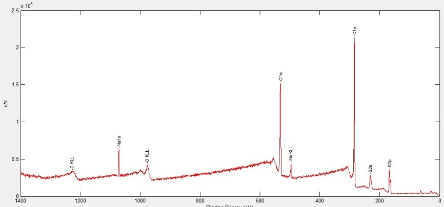
Analyse de surface ESCA : scan XPS

Diffraction of a beam of X-ray photons

Détails : site web du groupe EPIPHY

The diffraction of a beam of X-ray photons by a crystal allows a fine analysis of its structure. The IEMN is equipped to analyze the physical structure of single crystal semiconductor materials. A PANalytical X'Pert Pro MRD goniometer with double X-ray diffraction allows us to measure important parameters in the field of epitaxial growth such as the lattice parameter, the composition of alloys or the relaxation rate of a constrained crystal.

This system allows non-destructive testing of samples mounted on an x-y table accepting substrates up to 100 mm in diameter. Main applications:

  •  measurements of alloy compositions and layer thicknesses
  •  control of the adaptation in mesh parameter with the substrate
  •  quality of interfaces in super networks
  •  constrained thin films
  •  relaxation rate and tilt of mismatched thick layers

Scanning Electron Microscopy (SEM)

In terms of observation and validation of nanometric processes in the laboratory, our scanning electron microscopes (Zeiss Ultra55/EDS Bruker, Zeiss Supra55VP/EBSD Oxford) allow us to observe and dimension devices, whose size is in the order of ten nanometers. The observation of surface or cleaved section is possible on any type of insulating materials (resins, oxides or nitrides) or conductors (Si or III/V substrates, metallizations,...). The range of acceleration voltages (200V to 30kV) allows all observations without metallization during the process.

Energy dispersive spectroscopy (EDS)

Système EDS Xflash 4010 Bruker, type SDD (Silicon Drift Detector)

Catacteritics

  • Résolution du Mn Ka à 127 eV  de 0 à 100 000 cps
  • Qualitative
  • Quantitative
  • Mapping
Analyse chimique élémentaire par EDS

Analyse chimique élémentaire par EDS

Electron Backscatter Diffraction (EBSD)

The IEMN is also equipped with an EBSD (electron backscatter diffraction) detector on one of its scanning electron microscopes for the determination of the local orientation on crystalline material. We can thus carry out quantitative analyses by mapping microstructures, evaluate the orientations of crystallized films, map disorientations,...

  • CMNF - Micro and Nano Fabrication Center
    • CMNF Staff
    • Deposits and epitaxy division
      • Chemical Vapour Deposition (CVD)
      • Physical Vapour Deposition (PVD)
      • Inkjet printing
      • Heat tratments
      • Chemical synthesis and surface functionalisation
      • Epitaxial growth
    • Lithography Unit
      • Electronic Lithography
      • Optic Lithography
      • 2D laser lithography
      • Collage
    • Engraving and implantation pole
      • Etching and plasma treatment
      • Deep etching of silicon
      • Chemical vapor etching
      • Ion beam etching
      • Focused Ion Beam
      • Ion implantation
      • Wet etching and surface preparation
    • In Line Analysis Unit
      • Structural characterizations
      • Electrical properties
      • Propriétés optiques et spectroscopies
      • Microscopy Topography Morphology
      • Faisceau / beam
    • Soft Lithography and Bio Microfluidics
      • Soft lithography
      • BioMicroFluidics
    • Packaging Division
      • Shaping chips and wafers
      • Component assembly
      • Precision machining
  • PCMP - Multi-Physics Characterization Platform
    • PCMP Staff
    • Scanning Probe Microscopy Facility
      • Air Domain
      • UHV domain
    • Hyperfrequency, Optical and Photonic Characterization (CHOP)
      • Spectroscopy
      • Static - Small signal - Noise
      • Power
      • Nano characterisation
      • MEMS
      • Microwave photonics
      • Millimetre and THz
      • Temperature measurements
    • Characterisation of COMmunicating Systems and Prototyping cluster (SigmaCOM)
      • Analog and digital communication systems
        • Energy efficiency test bench
        • Multifunctional analogue and digital I/O devices
        • Software-defined radio
        • Telecom test bench
      • Optical communication systems
      • Prototypage (SigmaCom – C2EM)
        • Design Modelling
        • Programming
        • Achievements
        • Tests & Measurements
    • Characterisation, ElectroMagnetic Compatibility and Prototyping Centre (C2EM)
      • Anechoic chamber
      • TEM cell
      • Reverberation chamber with mode mixing
      • MaMIMOSA
      • Measurement Zt
  • Services offered by our platforms
    • services of the Bio Micro Fluidic platform
    • Services of the CMNF platform
Logo
Cité Scientifique
Avenue Henri Poincaré
CS 60069
59 652 Villeneuve d'Ascq Cedex, France
Tel : 03 20 19 79 79
CNRS Logo University of Lille Logo University Polytech Logo Junia Logo Centrale Lille Logo Renatech Logo RFnet Logo
Site map
Copyright Service ECM et pôle SISR 2024
  • Scientific production
  • Legal information
  • Privacy policy
Faire défiler vers le haut
fr_FR
fr_FR
en_GB
We use cookies to ensure you have the best experience on our website. If you continue to use this site, we will assume that you are happy with it.OKNoPrivacy policy