

MEMS
 Les performances d’actionneurs basés sur des effets électrostatiques, thermiques ou piézoélectriques peuvent être mesurées. Cela grâce à une station sous
pointes dédiée permettant la mesure des déplacements des actionneurs mais également via un impédancemètre , une enceinte d’accélérométrie sous vide,
un vibromètre laser ou encore, un AFM dédié au test de pointes MEMS.
Contact: Marc FAUCHER marc.faucher@isen.iemn.univ-lille1.fr 03 20 19 79 47
Didier THERON didier.theron@iemn.univ-lille1.fr 03 20 19 78 26
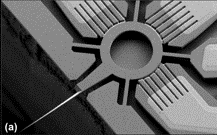
 Laser Vibrometer
Visualiser les déformations de surface, connaitre la vitesse, la fréquence et la distance de déplacement d’un élément vibrant, sont des informations primordiales des structures MEMs. Notre vibromètre permet de mesurer des déplacements inférieurs au picomètre pour une fréquence maximum de 24MHz.
Contact:
Abdelkrim TALBI Abdelkrim.Talbi@iemn.univ-lille1.fr 03 20 19 79 46
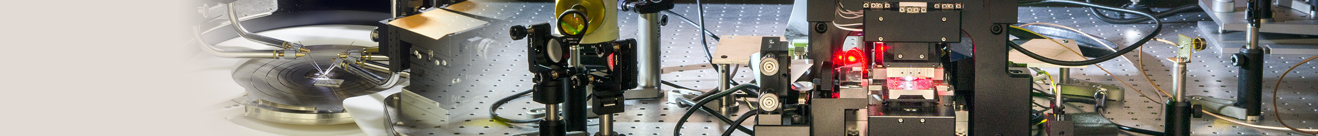
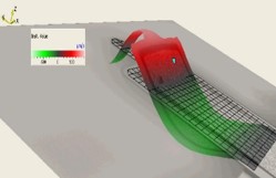
AFM Smart
Les sondes pour l’AFM sont un élément essentiel pour l’imagerie. Selon les propriétés de la sonde (fréquence, raideur) les modes d’imagerie peuvent varier fortement. Nous nous intéressons à la réalisation de sondes innovantes en technologie MEMS fonctionnant à haute fréquence (quelques dizaines de MHz).
Celles-ci sont actuellement commercialisées par la société Vmicro. Ces sondes sont ensuite testées sur un AFM commercial Bruker multimode à l’aide d’une interface spécifique. Pour tester les sondes MEMS destinés à l’AFM, l’IEMN dispose de 2 AFMs commerciaux Bruker multimode. Ces AFMs sont instrumentés spécifiquement pour leur permettre de fonctionner avec ces sondes. Nous avons développé en collaboration avec Keysight Technologies une interface spécifique utilisant un signal hyperfréquence.
Contact: Marc FAUCHER marc.faucher@isen.iemn.univ-lille1.fr 03 20 19 79 47
Didier THERON didier.theron@iemn.univ-lille1.fr 03 20 19 78 26


