
Notre savoir faire comprend la gravure des matériaux III/V divers,divers alliages tels que TaN, TiN, diélectriques, des matériaux magnétiques ou encore ferroélectriques et les traitements et préparations de surface.
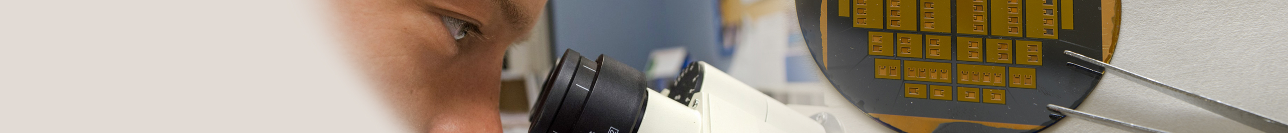
Pour réaliser ces gravures, nous avons à notre disposition, 2 systèmes RIE Plasmalab 80+ (Oxford), un système ICP-RIE system Plasmalab 100 (Oxford) à 2 chambres et un système ICP-RIE de la marque Sentech. Un grand nombre de matériaux peut être gravé grâce à la diversité de gaz disponibles: N2, O2, Ar, He, SF6, C4F8, CHF3, CH4, H2, CF4, BCl3, Cl2. Des wafers de 4 pouces sont utilisés mais il est possible par simple collage sur un wafer support de graver des morceaux.
Nous utilisons également les plasmas RF O2 pour les traitements et préparations de surface, ainsi qu’un stripper (PVA Tepla 300) pour les gravures et préparations de surface par plasma micro-ondes de O2/CF4 .
Expertise and know-how: some highlights
- Controlled etching of III/V materials such as GaAs, InP, InGaAs, GaSb, GaN,... by ICP in a chlorinated medium.
Realization of a GaSb based I-MOSFET (Anode team)
- Control through a comparative study of the selectivity of e-beam resins (PMMA, ZEP, CSAR) in ICP or RIE plasmas of SF6 or Cl2 chemistry

Behavior of ZEP resin during 50 nm pitch 150 nm trench etching (collaborative study of lithography and etching resources).
- Etching of multilayer magneto-electric assemblies

Etching of a PMN-PT microstructure by plasma ICP-RIE Chlorine (Aiman-films group)
Expertise and know-how: other
- Surface treatments and cleaning by O2, SF6/O2 or Ar/O2 plasma
- Surface preparation before anodic or thermal bonding by microwave O2 plasma
- Silicon etching in RIE and ICP-RIE, including Si nanowire formation,...
- Deburring and de-flashing of etching flanks after Bosch process to improve component performance without scaloping
Contacts: Timothey Bertrand, Giuseppe Di Gioia, Dmitri Yarekha


