IEMN
  • Home
  • News
    • IEMN Newsletters
    • M2-Ingé Internships
    • Job offers
    • All news
  • The Institute
    • Presentation
    • Organization of the institute
    • The Scientific Department
    • The Technological Department
    • Administrative and financial management
    • Rules of procedure
    • Our commitments
  • The Research
    • Scientific departments
      • Nanostructured Materials and Components
      • Micro / nano optoelectronics
      • Telecommunications Technologies and Intelligent Systems
      • Acoustic
    • Research groups
    • Flagship
  • Scientific Production
    • IEMN publications
    • Scientific production resources
  • The platforms
    • CMNF - Central Platform for Micro Nano Manufacturing
      • Engraving and implantation pole
      • In Line Analysis Unit
      • Soft Lithography and Bio Microfluidics
      • Deposits and epitaxy division
      • Lithography Unit
      • Packaging Division
      • CMNF Staff
    • PCMP - Multi-Physics Characterization Platform
      • Scanning Probe Microscopy Facility
      • Hyperfrequency, Optical and Photonic Characterization (CHOP)
      • Advanced Communications Systems and Prototyping cluster (SigmaCOM)
      • Characterisation, ElectroMagnetic Compatibility and Prototyping Centre (C2EM)
      • PCMP Staff
    • Services offered by our platforms
  • Partnership - Valuation
    • Academic Collaborations
    • ANR Projects
    • Main international collaborations
    • Industrial partnerships
    • The joint IEMN-Industry laboratories
    • Startups
  • Research Training
    • After the thesis
      • Do a post-doc at the IEMN
      • Towards the world of business and industry
      • Become a teacher-researcher
      • Become a Researcher
      • Starting a business at IEMN
      • FOCUS on a SATT engineer from the IEMN
    • A thesis at IEMN
      • Thesis and HDR defenses
      • Thesis topics
      • Financing
      • Doctoral studies
    • Master - Engineer
      • Masters ULille
        • Master Life Sciences and Technologies graduate programme
        • Master Nanosciences and Nanotechnologies - Speciality ETECH
        • Master Networks and Telecommunications
      • UPHF-INSA Masters
        • Master in Embedded Systems and Mobile Communications Engineering
        • Master Cyber Defense and Information Security
        • Master in Materials, Control and Safety
        • Master in Image and Sound Systems Engineering
      • Partner/Tutoring Engineering Schools
      • M2-Ingé Internships
    • The Lille branch of the GIP-CNFM
    • Nano-École Lille
  • Contact Us
    • Location
    • Contact form
    • Annuaire Intranet
  • Our support
  • fr_FR
  • Rechercher
  • Menu Menu
PLATEFORME : CENTRALE DE MICRO NANO FABRICATION
Slide thumbnailPLATEFORME : CENTRALE DE MICRO NANO FABRICATION
PLATEFORME : CENTRALE DE MICRO NANO FABRICATION

Physical Vapour Deposition (PVD)

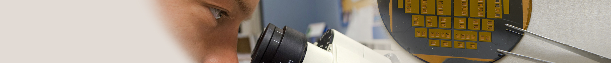
Nous nous appuyons principalement sur deux techniques de dépôt physique en phase vapeur qui sont l’évaporation et la pulvérisation cathodique, pour proposer des métaux pour électrodes, contacts ohmiques, épaississements, collage direct de substrat, écoulement des charges au masqueur, des multicouches de matériaux magnétiques et multi-ferroïques nanostructurées, des nitrures de métaux de transition pour électrodes et électrodes capacitives, des isolants et des semiconducteurs. Les caractéristiques et propriétés de ces matériaux sont utilisées dans les domaines suivants :

-Le microstockage de l’énergie (microsupercondensateur pour l’IOT, microcondensateur hybride tout solide pour l’électronique haute tension, microbatterie)

-La micro et nanoélectronique, photonique THz et optoélectronique des filières IIIV, GaN ou Si

-Les MEMS/NEMS Si et GaN, les bioMEMS et la microfluidique

-La spintronique THz et les dispositifs magnéto-acoustiques

Grâce au CPER IMITECH et à l’EQUIPEX+ NANOFUTUR, l’activité PVD du pôle s’est renforcée avec une nouvelle machine de pulvérisation cathodique magnétron de 12 cathodes équipée de générateurs HIPIMS, DC pulsé et RF.

Expertise, savoir-faire

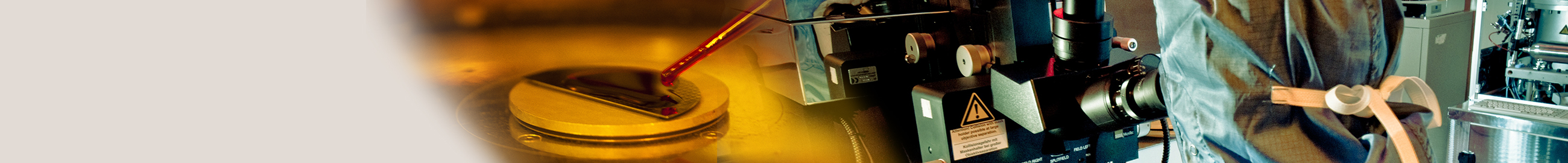
L’évaporation est réalisée avec un canon à électrons (PLASSYS MEB 550SL + 2 MEB 550S à 4 satellites) ou par effet joule (PLASSYS MEB 450S) sur une large gamme de métaux : Au, Ti, Ge, Al, Pt, Ni, Mo, Cr, Pd, Ag et In. Les options permettent de déposer en rotation planétaire pour améliorer l’uniformité, sous angle pour assurer la continuité de dépôt sur des marches et d’effectuer des décapages à l’Ar pour améliorer l’adhérence ou graver de très fines couches (quelques nm). Selon les équipements, les dépôts sont possibles sur des échantillons allant du morceau jusqu’à 150mm.

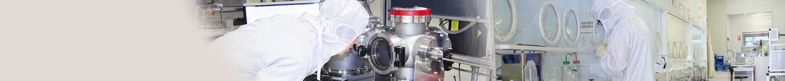
La pulvérisation cathodique magnétron est disponible sur 7 chambres de dépôt (ALLIANCE CONCEPT 2 DP650 + cluster CT200 3 chambres, ELETTRORAVA et LEYBOLD Z550 (contact N. Tiercelin)).  Sur l’ensemble de notre parc, nous disposons d’une trentaine de cathodes planaires ou confocales du 50mm au 100mm, de gaz Ar, N2 et O2 pour les mélanges réactifs, de générateurs HIPIMS, DC pulsé et RF utilisables également en copulvérisation, de postes froids et chauds (450°C, 600°C et 800°C). Nous pouvons déposer sur des échantillons allant du morceau jusqu’à jusqu’à 100mm et nous possédons une centaine de cibles. Les matériaux déposés sont : Au, Al, Bi, Ti, Cr, Ni, W, Cu, Pt, Mo, TiN, VN, WN, RuN, TaN, Ta2O5, TiO2, Nb2O5, ITO… et des couches magnétiques telles que TbFe2, TbCo2, TbFeCo, FeCo, Fe, CoPt, FePt …

some examples

– Film de RuN, de structure nanoplume, utilisé comme électrode dans les microsupercondensateurs. CV mesurée à 50mV/s dans un électrolyte aqueux.

1. Groupe CSAM, membre du RS2E, collaboration entre le CNRS, les universités de Lille, Nantes, Toulouse et de Califronie, et, le synchrotron Soleil. Nature materials 2024. Contact : C. Lethien


– Microcondensateurs électrolytiques à base de Tantale pour des applications à haute tension. Une étude comparative de deux empilements (Ta / Ta2O5 et TaN / Ta2O5) d’épaisseurs similaires (45 / 25 nm) agissant comme électrode de micro-condensateur électrolytique dans un électrolyte aqueux H2SO4 0,5M.

1. Groupe CSAM, membre du RS2E, collaboration entre le CNRS et l’université de Lille, Advanced materials 2024. Contact : C. Lethien


- Magnetic layer deposition by sputtering

Two sputtering frames are used for the deposition of metallic magnetic layers: A Leybold Z550 (RF, DC) and the Alliance Concept CT200 cluster chamber 1 (RF, DC, DC-pulse). The main materials deposited are transition metals (Fe, Co), alloys with rare earths (Tb, Sm, Gd) and combinations with non-magnetic buffers (Cu, Ru, Pt...). A particular know-how exists on the deposition of nanostructured magnetostrictive layers of type Nx[TbCo.2 (x nm)/FeCo (y nm). with controlled magnetic anisotropy. These stacks are used for applications such as magnetization control by magnetoelectric effect or coupling with surface acoustic waves.

1. Exemple de multicouche magnéto-élastique utilisée dans un capteur de champ magnétique à ondes acoustiques de surface (SAW). Contact N. Tiercelin groupe Aiman-films

- Electrochemical energy (micro) storage: materials for all-solid state lithium ion micro-batteries and micro-supercapacitors (thickness range 0.1 to 20 µm depending on the application). In the field of lithium ion micro-batteries, IEMN (CSAM group) has a recognized expertise on:

  • Titanium nitride lithium diffusion barrier deposit (TiN, bati Alliance concept 4 " DP650, Journal of the Electrochemical Society 2015)
  • the development of LiPON type solid electrolyte (> 1 µm, cluster CT 200, Material Chemistry and Physics 2010)
  • the development of high potential positive electrode in LiFePO4/C and LiMn1.5Ni0.5O4 (< 10 µm, cluster CT 200, Chem mat 2017 & ESM 2018)
  • the development of a negative electrode in Nb2O5 (< 3 µm, cluster CT 200)< 3 µm, cluster CT 200)

-micro-supercapacitor (CSAM group), the know-how is based on:

  • the development of metal carbide (TiC, < 20 µm, cluster CT 200, Science 2016, Electrochemica acta 2016, Journal of power sources 2016 & AFM 2017) for carbon/carbon micro-supercapacitors
  • the development of VN or WN transition metal nitride (< 10 µm, Cluster CT 200, Advanced Materials Technologies 2018) as pseudocapacitive electrode)

Contact: Jérémie Chaillou, Marc Dewitte, Carlos Moncasi-Luque, Isabelle Roch-Jeune – Pôle dépôt
Contact Leybold Z550 : Nicolas Tiercelin – Groupe AIMAN-FILMS

  • CMNF - Micro and Nano Fabrication Center
    • CMNF Staff
    • Deposits and epitaxy division
      • Chemical Vapour Deposition (CVD)
      • Physical Vapour Deposition (PVD)
      • Inkjet printing
      • Heat tratments
      • Chemical synthesis and surface functionalisation
      • Epitaxial growth
    • Lithography Unit
      • Electronic Lithography
      • Optic Lithography
      • 2D laser lithography
      • Collage
    • Engraving and implantation pole
      • Etching and plasma treatment
      • Deep etching of silicon
      • Chemical vapor etching
      • Ion beam etching
      • Focused Ion Beam
      • Ion implantation
      • Wet etching and surface preparation
    • In Line Analysis Unit
      • Structural characterizations
      • Electrical properties
      • Propriétés optiques et spectroscopies
      • Microscopy Topography Morphology
      • Faisceau / beam
    • Soft Lithography and Bio Microfluidics
      • Soft lithography
      • BioMicroFluidics
    • Packaging Division
      • Shaping chips and wafers
      • Component assembly
      • Precision machining
  • PCMP - Multi-Physics Characterization Platform
    • PCMP Staff
    • Scanning Probe Microscopy Facility
      • Air Domain
      • UHV domain
    • Hyperfrequency, Optical and Photonic Characterization (CHOP)
      • Spectroscopy
      • Static - Small signal - Noise
      • Power
      • Nano characterisation
      • MEMS
      • Microwave photonics
      • Millimetre and THz
      • Temperature measurements
    • Characterisation of COMmunicating Systems and Prototyping cluster (SigmaCOM)
      • Analog and digital communication systems
        • Energy efficiency test bench
        • Multifunctional analogue and digital I/O devices
        • Software-defined radio
        • Telecom test bench
      • Optical communication systems
      • Prototypage (SigmaCom – C2EM)
        • Design Modelling
        • Programming
        • Achievements
        • Tests & Measurements
    • Characterisation, ElectroMagnetic Compatibility and Prototyping Centre (C2EM)
      • Anechoic chamber
      • TEM cell
      • Reverberation chamber with mode mixing
      • MaMIMOSA
      • Measurement Zt
  • Services offered by our platforms
    • services of the Bio Micro Fluidic platform
    • Services of the CMNF platform
Logo
Cité Scientifique
Avenue Henri Poincaré
CS 60069
59 652 Villeneuve d'Ascq Cedex, France
Tel : 03 20 19 79 79
CNRS Logo University of Lille Logo University Polytech Logo Junia Logo Centrale Lille Logo Renatech Logo RFnet Logo
Site map
Copyright Service ECM et pôle SISR 2024
  • Scientific production
  • Legal information
  • Privacy policy
Faire défiler vers le haut
fr_FR
fr_FR
en_GB
We use cookies to ensure you have the best experience on our website. If you continue to use this site, we will assume that you are happy with it.OKNoPrivacy policy