
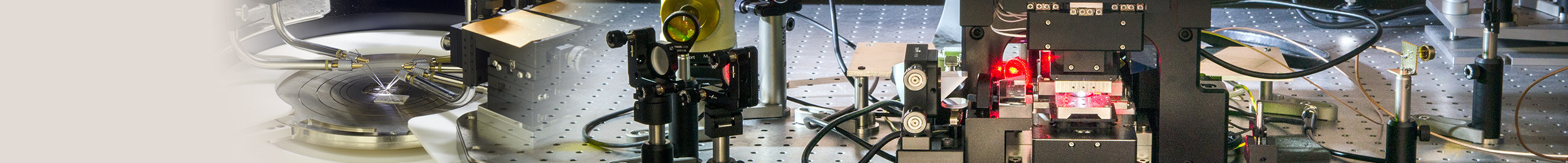

 Le pôle CHOP est équipé de nombreux instruments de mesures tels que alimentations programmables, analyseurs de réseaux vectoriels, mesureurs du facteur de bruit permettant d’effectuer la caractérisation statique et hyperfréquence jusque 110GHz en régime petit signal de composants (actifs ou passifs).
Statique
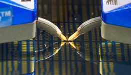
 Mesure incontournable pour tout composant électrique, les caractéristiques statiques s’effectuent avec une multitude d’équipement disponible. Les montages peuvent aussi se décliner sous plusieurs configuration que ce soit pour une étude de caractéristique ou pour alimenter des circuits complexes. Connectorisé ou sur tranche, d’une single probe aux pointes multicontacts (jusqu’à 32pins), nous pouvons effectué les caractéristiques statiques permettant d’identifier les performances et les disparités de fabrication ainsi que la robustesse des composants.
- i(V) jusqu’à 10kV
- en température
- i(V) pulsé sous vide
- C(V) à 40V, C(f) à 110MHz
- sous éclairement (mesures DC possible sous éclairement solaire ou laser)
 Petit signal
Pour faire un retour technologique dès la sortie de fabrication de la CMNF ou pour établir des schémas électriques équivalents de transistor pour le design de circuit complexe (convertisseur de fréquence, amplificateur, micro processor…) les mesures petit signal jusqu’à 110GHz sont au cœur de l’expertise du pôle CHOP. Ces mesures sont réalisées sous divers environnements contrôlés et configurations :
- Sur tranche en pulsé et en température
- En coaxial
- En guide d’onde
- En espace libre
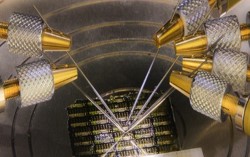
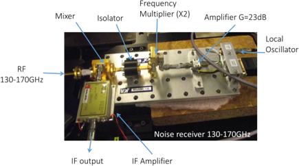 Facteur de Bruit
Pour l’extraction des quatre paramètres de bruit [gamma opt, Nfmin et Rn] de dispositifs semi-conducteur étudiés, le pôle CHOP dispose de plusieurs bancs de mesure automatisés permettant d’effectuer la mesure du gain disponible et du facteur de bruit (Noise Figure) de composants hyperfréquences sous pointes ou en boîtier selon les gammes de fréquences suivantes :
- 6-40GHz: NF50 et Tuner
- 75-110GHz: NF50
- 130-170GHz: NF50
- 170-260GHz: NF50 (en cours de développement)


