IEMN
  • Home
  • News
    • IEMN Newsletters
    • M2-Ingé Internships
    • Job offers
    • All news
  • The Institute
    • Presentation
    • Organization of the institute
    • The Scientific Department
    • The Technological Department
    • Administrative and financial management
    • Rules of procedure
    • Our commitments
  • The Research
    • Scientific departments
      • Nanostructured Materials and Components
      • Micro / nano optoelectronics
      • Telecommunications Technologies and Intelligent Systems
      • Acoustic
    • Research groups
    • Flagship
  • Scientific Production
    • IEMN publications
    • Scientific production resources
  • The platforms
    • CMNF - Central Platform for Micro Nano Manufacturing
      • Engraving and implantation pole
      • In Line Analysis Unit
      • Soft Lithography and Bio Microfluidics
      • Deposits and epitaxy division
      • Lithography Unit
      • Packaging Division
      • CMNF Staff
    • PCMP - Multi-Physics Characterization Platform
      • Scanning Probe Microscopy Facility
      • Hyperfrequency, Optical and Photonic Characterization (CHOP)
      • Advanced Communications Systems and Prototyping cluster (SigmaCOM)
      • Characterisation, ElectroMagnetic Compatibility and Prototyping Centre (C2EM)
      • PCMP Staff
    • Services offered by our platforms
  • Partnership - Valuation
    • Academic Collaborations
    • ANR Projects
    • Main international collaborations
    • Industrial partnerships
    • The joint IEMN-Industry laboratories
    • Startups
  • Research Training
    • After the thesis
      • Do a post-doc at the IEMN
      • Towards the world of business and industry
      • Become a teacher-researcher
      • Become a Researcher
      • Starting a business at IEMN
      • FOCUS on a SATT engineer from the IEMN
    • A thesis at IEMN
      • Thesis and HDR defenses
      • Thesis topics
      • Financing
      • Doctoral studies
    • Master - Engineer
      • Masters ULille
        • Master Life Sciences and Technologies graduate programme
        • Master Nanosciences and Nanotechnologies - Speciality ETECH
        • Master Networks and Telecommunications
      • UPHF-INSA Masters
        • Master in Embedded Systems and Mobile Communications Engineering
        • Master Cyber Defense and Information Security
        • Master in Materials, Control and Safety
        • Master in Image and Sound Systems Engineering
      • Partner/Tutoring Engineering Schools
      • M2-Ingé Internships
    • The Lille branch of the GIP-CNFM
    • Nano-École Lille
  • Contact Us
    • Location
    • Contact form
    • Annuaire Intranet
    • « Suivez-nous »
  • Our support
  • fr_FR
  • Rechercher
  • Menu Menu
CHOP : PÔLE CARACTERISATION HYPERFREQUENCE, OPTIQUE ET PHOTONIQUE

Spectroscopy

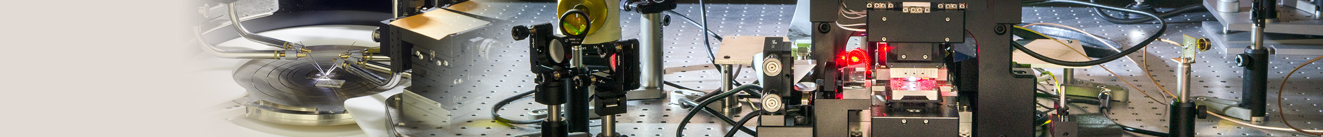
THz-TDS : SPECTROSCOPE TERAHERTZ EN DOMAINE TEMPOREL

La spectroscopie térahertz dans le domaine temporel est le dispositif de spectroscopie THz le plus répandu pour les mesures spectrales THz à large bande. Elle est basée sur un laser femtoseconde dont l’impulsion est transférée dans le domaine spectral THz grâce à une antenne photoconductrice (dans notre cas). L’impulsion THz résultante est ensuite échantillonnée dans le temps à l’aide d’une autre antenne photoconductrice déclenchée par le laser femtoseconde après un délai contrôlé. Cela conduit à des traces temporelles qu’une transformée de Fourier transfère dans le domaine spectral.

Application

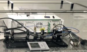
La THz-TDS est utilisée sur toutes sortes d’échantillons : gazeux, liquides, solides et même plasma. Elle permet de sonder les lignes rovibrationnelles des gaz avec une très bonne spécificité lorsque les molécules ont de ~3 à ~10 atomes. Elle est très sensible aux liquides polaires tels que l’eau et joue donc un rôle important en biologie. La spectroscopie THz à large bande est utilisée sur des échantillons de semi-conducteurs pour mesurer de très faibles niveaux de dopage et sur des cristaux moléculaires pour étudier leur conformation.

Etendue spectrale: 0,2 – 5 THz
Etendue totale de la trace temporelle: 850 ps
Résolution spectrale (limitée par la transformée de Fourier):  <1,2 GHz

Meilleure résolution possible par traitement du signal temporel
Dynamique : 100 dB
Type d’échantillons: solides (wafers, poudres, pastilles…) , particules resuspendues ou gaz

Contact:

Sophie.Eliet@univ-lille.fr
 
romain.peretti@univ-lille.fr

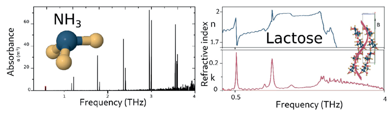
FTIR : SPECTROMÈTRE INFRAROUGE À TRANSFORMÉE DE FOURIER, COUPLÉ À UN MICROSCOPE

Ce FTIR purgé au N2 permet l’acquisition spectrale de l’IR moyen à la gamme spectrale THz
Gamme spectrale totale : 8 000 – 50 cm-1 (1,25μm- 200μm) (240THz- 1,5 THz)
Résolution spectrale : = 0,4 cm-1
Détecteurs : DLATGS interne 8000-350 cm-1 ; DTGS/PE interne 680-50 cm-1
MCT externe (refroidi à 77K) : 12000-600 cm-1
Source interne : Corps noir
Couplé à un microscope MIR et à un détecteur MCT interne (refroidi à 77K) : 12000-600 cm-1

Cartographie au microscope :

  • Précision du pas : 0,1μm
  • Répétabilité : 1μm
  • Précision du positionnement : +/-3μm

–

Spectroscopie exemple

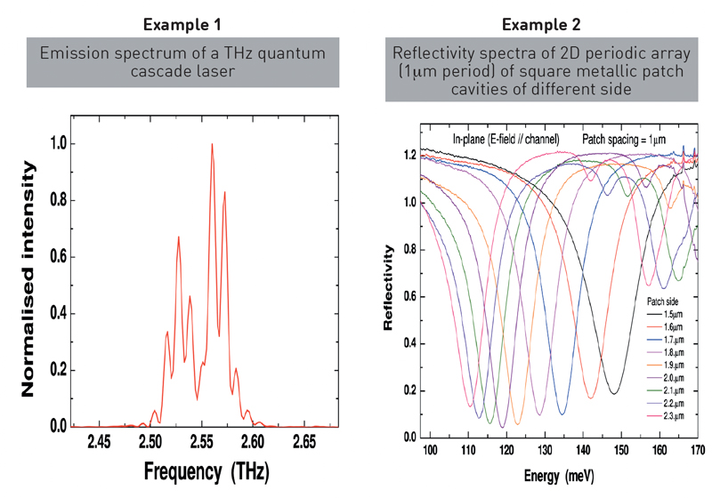
Les cavités sont constituées d’hétérostructures aGaAs/AlGAs et tissées entre le contact métallique et le plan de masse. Les spectres sont mesurés en géométrie de réflexion avec le microscope infrarouge moyen.

Contact:

Sophie.Eliet@univ-lille.fr
 
stefano.barbieri@univ-lille.fr

  • CMNF - Micro and Nano Fabrication Center
    • CMNF Staff
    • Deposits and epitaxy division
      • Chemical Vapour Deposition (CVD)
      • Physical Vapour Deposition (PVD)
      • Inkjet printing
      • Heat tratments
      • Chemical synthesis and surface functionalisation
      • Epitaxial growth
    • Lithography Unit
      • Electronic Lithography
      • Optic Lithography
      • 2D laser lithography
      • Collage
    • Engraving and implantation pole
      • Etching and plasma treatment
      • Deep etching of silicon
      • Chemical vapor etching
      • Ion beam etching
      • Focused Ion Beam
      • Ion implantation
      • Wet etching and surface preparation
    • In Line Analysis Unit
      • Structural characterizations
      • Electrical properties
      • Propriétés optiques et spectroscopies
      • Microscopy Topography Morphology
      • Faisceau / beam
    • Soft Lithography and Bio Microfluidics
      • Soft lithography
      • BioMicroFluidics
    • Packaging Division
      • Shaping chips and wafers
      • Component assembly
      • Precision machining
  • PCMP - Multi-Physics Characterization Platform
    • PCMP Staff
    • Scanning Probe Microscopy Facility
      • Air Domain
      • UHV domain
    • Hyperfrequency, Optical and Photonic Characterization (CHOP)
      • Spectroscopy
      • Static - Small signal - Noise
      • Power
      • Nano characterisation
      • MEMS
      • Microwave photonics
      • Millimetre and THz
      • Temperature measurements
    • Characterisation of COMmunicating Systems and Prototyping cluster (SigmaCOM)
      • Analog and digital communication systems
        • Energy efficiency test bench
        • Multifunctional analogue and digital I/O devices
        • Software-defined radio
        • Telecom test bench
      • Optical communication systems
      • Prototypage (SigmaCom – C2EM)
        • Design Modelling
        • Programming
        • Achievements
        • Tests & Measurements
    • Characterisation, ElectroMagnetic Compatibility and Prototyping Centre (C2EM)
      • Anechoic chamber
      • TEM cell
      • Reverberation chamber with mode mixing
      • MaMIMOSA
      • Measurement Zt
  • Services offered by our platforms
    • Prestations du pôle Bio Micro Fluidique – CMNF
    • Services of the CMNF platform
    • Cellule d’accueil projets Renatech
Logo
Cité Scientifique
Avenue Henri Poincaré
CS 60069
59 652 Villeneuve d'Ascq Cedex, France
Tel : 03 20 19 79 79
CNRS Logo University of Lille Logo University Polytech Logo Junia Logo Centrale Lille Logo Renatech Logo RFnet Logo
Site map
Copyright Service ECM et pôle SISR 2024
  • Scientific production
  • Legal information
  • Privacy policy
Faire défiler vers le haut
fr_FR
fr_FR
en_GB
We use cookies to ensure you have the best experience on our website. If you continue to use this site, we will assume that you are happy with it.