IEMN
  • Home
  • News
    • IEMN Newsletters
    • M2-Ingé Internships
    • Job offers
    • All news
  • The Institute
    • Presentation
    • Organization of the institute
    • The Scientific Department
    • The Technological Department
    • Administrative and financial management
    • Rules of procedure
    • Our commitments
  • The Research
    • Scientific departments
      • Nanostructured Materials and Components
      • Micro / nano optoelectronics
      • Telecommunications Technologies and Intelligent Systems
      • Acoustic
    • Research groups
    • Flagship
  • Scientific Production
    • IEMN publications
    • Scientific production resources
  • The platforms
    • CMNF - Central Platform for Micro Nano Manufacturing
      • Engraving and implantation pole
      • In Line Analysis Unit
      • Soft Lithography and Bio Microfluidics
      • Deposits and epitaxy division
      • Lithography Unit
      • Packaging Division
      • CMNF Staff
    • PCMP - Multi-Physics Characterization Platform
      • Scanning Probe Microscopy Facility
      • Hyperfrequency, Optical and Photonic Characterization (CHOP)
      • Advanced Communications Systems and Prototyping cluster (SigmaCOM)
      • Characterisation, ElectroMagnetic Compatibility and Prototyping Centre (C2EM)
      • PCMP Staff
    • Services offered by our platforms
  • Partnership - Valuation
    • Academic Collaborations
    • ANR Projects
    • Main international collaborations
    • Industrial partnerships
    • The joint IEMN-Industry laboratories
    • Startups
  • Research Training
    • After the thesis
      • Do a post-doc at the IEMN
      • Towards the world of business and industry
      • Become a teacher-researcher
      • Become a Researcher
      • Starting a business at IEMN
      • FOCUS on a SATT engineer from the IEMN
    • A thesis at IEMN
      • Thesis and HDR defenses
      • Thesis topics
      • Financing
      • Doctoral studies
    • Master - Engineer
      • Masters ULille
        • Master Life Sciences and Technologies graduate programme
        • Master Nanosciences and Nanotechnologies - Speciality ETECH
        • Master Networks and Telecommunications
      • UPHF-INSA Masters
        • Master in Embedded Systems and Mobile Communications Engineering
        • Master Cyber Defense and Information Security
        • Master in Materials, Control and Safety
        • Master in Image and Sound Systems Engineering
      • Partner/Tutoring Engineering Schools
      • M2-Ingé Internships
    • The Lille branch of the GIP-CNFM
    • Nano-École Lille
  • Contact Us
    • Location
    • Contact form
    • Annuaire Intranet
  • Our support
  • fr_FR
  • Rechercher
  • Menu Menu
CHOP : PÔLE CARACTERISATION HYPERFREQUENCE, OPTIQUE ET PHOTONIQUE
Slide thumbnailCHOP : PÔLE CARACTERISATION HYPERFREQUENCE, OPTIQUE ET PHOTONIQUE
CHOP : PÔLE CARACTERISATION HYPERFREQUENCE, OPTIQUE ET PHOTONIQUE

Microwave photonics

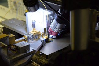
The microwave optoelectronics characterisation bench consists mainly of a display system and positioners for dynamic electrical characterisation of (opto-) electronic components under constant or modulated power optical illumination. Using the instrumentation available on the platform, it is possible on this bench, for example, to :

  • measure the electrical characteristics of components under continuous illumination in the form of a small signal (S parameter) up to 320 GHz
  • measure component noise under continuous illumination up to 50 GHz
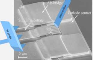
  • frequency characterisation of the photoresponse of fast photodetectors. The optical wavelengths accessible are around 400 nm, 800 nm, 1000 nm, 1300 nm and 1550 nm.

A femto second laser with a high repetition rate can also be used to carry out measurements with a sampling rate of 1 GHz.

Contacts:

Emilien.peytavit@univ-lille.fr
 
Sophie.eliet@univ-lille.fr

  • CMNF - Micro and Nano Fabrication Center
    • CMNF Staff
    • Deposits and epitaxy division
      • Chemical Vapour Deposition (CVD)
      • Physical Vapour Deposition (PVD)
      • Inkjet printing
      • Heat tratments
      • Chemical synthesis and surface functionalisation
      • Epitaxial growth
    • Lithography Unit
      • Electronic Lithography
      • Optic Lithography
      • 2D laser lithography
      • Collage
    • Engraving and implantation pole
      • Etching and plasma treatment
      • Deep etching of silicon
      • Chemical vapor etching
      • Ion beam etching
      • Focused Ion Beam
      • Ion implantation
      • Wet etching and surface preparation
    • In Line Analysis Unit
      • Structural characterizations
      • Electrical properties
      • Propriétés optiques et spectroscopies
      • Microscopy Topography Morphology
      • Faisceau / beam
    • Soft Lithography and Bio Microfluidics
      • Soft lithography
      • BioMicroFluidics
    • Packaging Division
      • Shaping chips and wafers
      • Component assembly
      • Precision machining
  • PCMP - Multi-Physics Characterization Platform
    • PCMP Staff
    • Scanning Probe Microscopy Facility
      • Air Domain
      • UHV domain
    • Hyperfrequency, Optical and Photonic Characterization (CHOP)
      • Spectroscopy
      • Static - Small signal - Noise
      • Power
      • Nano characterisation
      • MEMS
      • Microwave photonics
      • Millimetre and THz
      • Temperature measurements
    • Characterisation of COMmunicating Systems and Prototyping cluster (SigmaCOM)
      • Analog and digital communication systems
        • Energy efficiency test bench
        • Multifunctional analogue and digital I/O devices
        • Software-defined radio
        • Telecom test bench
      • Optical communication systems
      • Prototypage (SigmaCom – C2EM)
        • Design Modelling
        • Programming
        • Achievements
        • Tests & Measurements
    • Characterisation, ElectroMagnetic Compatibility and Prototyping Centre (C2EM)
      • Anechoic chamber
      • TEM cell
      • Reverberation chamber with mode mixing
      • MaMIMOSA
      • Measurement Zt
  • Services offered by our platforms
    • services of the Bio Micro Fluidic platform
    • Services of the CMNF platform
Logo
Cité Scientifique
Avenue Henri Poincaré
CS 60069
59 652 Villeneuve d'Ascq Cedex, France
Tel : 03 20 19 79 79
CNRS Logo University of Lille Logo University Polytech Logo Junia Logo Centrale Lille Logo Renatech Logo RFnet Logo
Site map
Copyright Service ECM et pôle SISR 2024
  • Scientific production
  • Legal information
  • Privacy policy
Faire défiler vers le haut
fr_FR
fr_FR
en_GB
We use cookies to ensure you have the best experience on our website. If you continue to use this site, we will assume that you are happy with it.OKNoPrivacy policy