IEMN
  • Home
  • News
    • IEMN Newsletters
    • M2-Ingé Internships
    • Job offers
    • All news
  • The Institute
    • Presentation
    • Organization of the institute
    • The Scientific Department
    • The Technological Department
    • Administrative and financial management
    • Rules of procedure
    • Our commitments
  • The Research
    • Scientific departments
      • Nanostructured Materials and Components
      • Micro / nano optoelectronics
      • Telecommunications Technologies and Intelligent Systems
      • Acoustic
    • Research groups
    • Flagship
  • Scientific Production
    • IEMN publications
    • Scientific production resources
  • The platforms
    • CMNF - Central Platform for Micro Nano Manufacturing
      • Engraving and implantation pole
      • In Line Analysis Unit
      • Soft Lithography and Bio Microfluidics
      • Deposits and epitaxy division
      • Lithography Unit
      • Packaging Division
      • CMNF Staff
    • PCMP - Multi-Physics Characterization Platform
      • Scanning Probe Microscopy Facility
      • Hyperfrequency, Optical and Photonic Characterization (CHOP)
      • Advanced Communications Systems and Prototyping cluster (SigmaCOM)
      • Characterisation, ElectroMagnetic Compatibility and Prototyping Centre (C2EM)
      • PCMP Staff
    • Services offered by our platforms
  • Partnership - Valuation
    • Academic Collaborations
    • ANR Projects
    • Main international collaborations
    • Industrial partnerships
    • The joint IEMN-Industry laboratories
    • Startups
  • Research Training
    • After the thesis
      • Do a post-doc at the IEMN
      • Towards the world of business and industry
      • Become a teacher-researcher
      • Become a Researcher
      • Starting a business at IEMN
      • FOCUS on a SATT engineer from the IEMN
    • A thesis at IEMN
      • Thesis and HDR defenses
      • Thesis topics
      • Financing
      • Doctoral studies
    • Master - Engineer
      • Masters ULille
        • Master Life Sciences and Technologies graduate programme
        • Master Nanosciences and Nanotechnologies - Speciality ETECH
        • Master Networks and Telecommunications
      • UPHF-INSA Masters
        • Master in Embedded Systems and Mobile Communications Engineering
        • Master Cyber Defense and Information Security
        • Master in Materials, Control and Safety
        • Master in Image and Sound Systems Engineering
      • Partner/Tutoring Engineering Schools
      • M2-Ingé Internships
    • The Lille branch of the GIP-CNFM
    • Nano-École Lille
  • Contact Us
    • Location
    • Contact form
    • Annuaire Intranet
  • Our support
  • fr_FR
  • Rechercher
  • Menu Menu
PLATEFORME : CENTRALE DE MICRO NANO FABRICATION
Slide thumbnailPLATEFORME : CENTRALE DE MICRO NANO FABRICATION
PLATEFORME : CENTRALE DE MICRO NANO FABRICATION

Optic Lithography

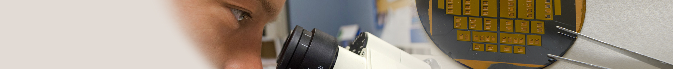
La zone photolithographie est équipée de 2 aligneurs de masques optiques MA6/BA6 (6 inch) N°750 et 834 de marque Suss MicroTec.

Passage de la génération GEN 2 à GEN 4 permettant la continuité des maintenances curatives et préventives sur plus de 7 ans.

Résolution < 1µm en mode vacuum contact et en alignement face avant TSA < 0,5 µm. Résolution < 1µm en mode Vacuum contact et alignement face arriere BSA < 1 µm Acquisition Video pour alignement wafer / masque en TSA / BSA Portes Wafer: 1/4, 1/2 de 2", 2", 3", 4" avec portes masques optiques 4", 5". Démarche éco-responsable, avec une baisse de la consommation d'énergie, de l’azote et de l’air comprimé consommées et passage en UV LED qui permettra la suppression des lampes à mercure nocives pour l’environnement et très coûteuses. UV-LED: 10 000 Heures de fonctionnement. [/av_textblock] [/av_two_third][av_heading heading='Expertises et savoir-faire: quelques points marquants' tag='h6' link_apply='' link='' link_target='' style='' size='' subheading_active='' subheading_size='15' margin='' padding='15' color='' custom_font='' custom_class='' admin_preview_bg='' av-desktop-hide='' av-medium-hide='' av-small-hide='' av-mini-hide='' av-medium-font-size-title='' av-small-font-size-title='' av-mini-font-size-title='' av-medium-font-size='' av-small-font-size='' av-mini-font-size='' av_uid='av-3tmbpm'][/av_heading] [av_three_fifth first min_height='' vertical_alignment='' space='' custom_margin='' margin='0px' padding='0px' border='' border_color='' radius='0px' background_color='' src='' background_position='top left' background_repeat='no-repeat' animation='' av_uid='av-zcavju'] [av_textblock size='' font_color='' color='' av_uid='av-yazfcq'] - Technologie pont à air métallique par électrolyse (2 à 5µm) à l’aide d’un bicouche de résine.


[/av_three_fifth]

 1.  Air bridge, 2µm Au electrolysis (optoelectronics team)

- Cap layer sorting for lift off of metal deposits made by sputtering

2. Lift off of a 3µm Au deposit made by sputtering (NAM6 team)

- Thick resins (SPR, AZ15NXT) for making very deep engravings up to Via-hole by deep dry etching process

3. High aspect ratio structures SPR220 4µm on Si (CSAM team)


Expertise and know-how: other
  • Production of structured resin masks (from 300 nm to some 40 µm thick) for dry etching (ICP, RIE, DRIE, RIBE) or wet etching of materials.
  • Realization of bi or trilayers of resins as protective masks for implantation, for metallic deposits (evaporation or spraying by the lift-off technique), for electrolysis (Au, Cu, ...)
  • Realization of specific annealing with control of the temperature ramps allowing to minimize the constraints in the polymer or for the transfer of materials (graphene, parylene,...).
  • Use of thick resins (3 to 5µm) as front protection during mechanical or laser cutting.
  • CMNF - Micro and Nano Fabrication Center
    • CMNF Staff
    • Deposits and epitaxy division
      • Chemical Vapour Deposition (CVD)
      • Physical Vapour Deposition (PVD)
      • Inkjet printing
      • Heat tratments
      • Chemical synthesis and surface functionalisation
      • Epitaxial growth
    • Lithography Unit
      • Electronic Lithography
      • Optic Lithography
      • 2D laser lithography
      • Collage
    • Engraving and implantation pole
      • Etching and plasma treatment
      • Deep etching of silicon
      • Chemical vapor etching
      • Ion beam etching
      • Focused Ion Beam
      • Ion implantation
      • Wet etching and surface preparation
    • In Line Analysis Unit
      • Structural characterizations
      • Electrical properties
      • Propriétés optiques et spectroscopies
      • Microscopy Topography Morphology
      • Faisceau / beam
    • Soft Lithography and Bio Microfluidics
      • Soft lithography
      • BioMicroFluidics
    • Packaging Division
      • Shaping chips and wafers
      • Component assembly
      • Precision machining
  • PCMP - Multi-Physics Characterization Platform
    • PCMP Staff
    • Scanning Probe Microscopy Facility
      • Air Domain
      • UHV domain
    • Hyperfrequency, Optical and Photonic Characterization (CHOP)
      • Spectroscopy
      • Static - Small signal - Noise
      • Power
      • Nano characterisation
      • MEMS
      • Microwave photonics
      • Millimetre and THz
      • Temperature measurements
    • Characterisation of COMmunicating Systems and Prototyping cluster (SigmaCOM)
      • Analog and digital communication systems
        • Energy efficiency test bench
        • Multifunctional analogue and digital I/O devices
        • Software-defined radio
        • Telecom test bench
      • Optical communication systems
      • Prototypage (SigmaCom – C2EM)
        • Design Modelling
        • Programming
        • Achievements
        • Tests & Measurements
    • Characterisation, ElectroMagnetic Compatibility and Prototyping Centre (C2EM)
      • Anechoic chamber
      • TEM cell
      • Reverberation chamber with mode mixing
      • MaMIMOSA
      • Measurement Zt
  • Services offered by our platforms
    • services of the Bio Micro Fluidic platform
    • Services of the CMNF platform
Logo
Cité Scientifique
Avenue Henri Poincaré
CS 60069
59 652 Villeneuve d'Ascq Cedex, France
Tel : 03 20 19 79 79
CNRS Logo University of Lille Logo University Polytech Logo Junia Logo Centrale Lille Logo Renatech Logo RFnet Logo
Site map
Copyright Service ECM et pôle SISR 2024
  • Scientific production
  • Legal information
  • Privacy policy
Faire défiler vers le haut
fr_FR
fr_FR
en_GB
We use cookies to ensure you have the best experience on our website. If you continue to use this site, we will assume that you are happy with it.OKNoPrivacy policy