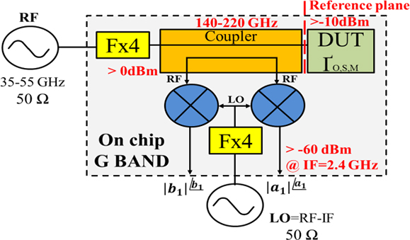
Microelectronic application such as wireless communication, radar or space detection require higher data rate resolutions, implying the use of millimeter wave and submillimeter frequencies. Thanks to the silicon technologies improvement, some microelectronic circuits are emerging working in the frequency range of 140-220 GHz (G-band) but they suffer from a lack of complete characterization tools involving costly investment and limitations due to the loss between the measurement setups and the devices under test (DUT). Therefore, measurement setups integrated with the DUT (VNA 1 port and 2 ports) have been designed processed and measured in BiCMOS technology. Fig.2 shows the schematic (Fig.2a) and the dice (Fig.2b) of the one port in situ measurement system permitting measurement from 160-200GHz with an usual VNA (fmax =55GHz). The results are very promising. Before this, each blocks have been designed and measured in standalone, reaching state of the art results [1-3].
In the future, we plan to pursue this activity by integrating these mmW and sub mmW in microwave probes in order to obtain functionalize probes allowing Sij measurements but also, noise and power measurement thanks to noise source, noise receiver, power detector and tuner associated in these probes. These elements in standalone have been validated. A specific focus will be given to packaging, probe technologies development and design will be achieved in collaboration with Equipex Excelsior for micro or nanoprobing aspects and LEAF for packaging.
[1] GAUTHIER A. et al, BCTM 2017, Miami, FL, USA, October 2017
[2] AOUIMEUR W. et al, SiRF 2017, Phoenix, AZ, USA, January 2017
[3] BOSSUET A et al, IEEE Microw. Wirel. Compon. Lett. 26, 11, November 2016


