
AGAMI_EURIGAMI (EUROPEAN DEFENCE FUND)
AGAMI_EURIGAMI :
European Innovative GaN Advanced Microwave Integration - European project EDF (EUROPEAN DEFENCE FUND)
- IEMN Project Sponsor: F. Medjdoub
- Coordinator: UMS GmbH
- Partners: Fraunhofer IAF, Fraunhofer IZM, UMS SAS, CEA LETI, 3-5 Lab, University of Roma Tor Vergata, MC2, University of Vigo, Universidad Politécnica de Madrid, University Zagreb, SOITEC, SweGaN, Sencio, IMT Bucharest, Slovak Academy of Science (SAV), Chalmers University, FORTH, Leonardo, Synergie CAD, Hensoldt, Indra, MEC, Thales NL, Thales DMS, University of Roma La Sapienza, BPTI, Saab, University Padova, Circuit Integrated Ltd., Airbus-Spain, National Research Council, CNRS-IEMN, TNO, Elettronica

The project “European Innovative GaN Advanced Microwave Integration” (AGAMI_EURIGAMI) covers the complete supply chain for Gallium Nitride (GaN) starting from epitaxy up to the component packaging and integration in modern electronic defence systems. The project focusses on the improvement of the technology and of the resilience against electrical and environmental threats. The final GaN components and devices will demonstrate an improved performance and protection of the devices in harsh environments.
The main technological or characterization means that will be necessary to carry out the project:
- CNMF : Centrale de micro et nano fabrication
- Plateforme CHOP : caractérisation DC, pulsée, RF, non-linéaire (Load-pull)
Flagship projects concerned:
- Telecom UHD
- Micro-nano-devices
ACTION (ANR PRCE)
ACTION :
Novel AlGaN channel transistors for high voltage applications
- IEMN Project Sponsor: F. Medjdoub
- Coordinator: IEMN
- Partners: Institut Néel, société EasyGaN, laboratoire CRHEA
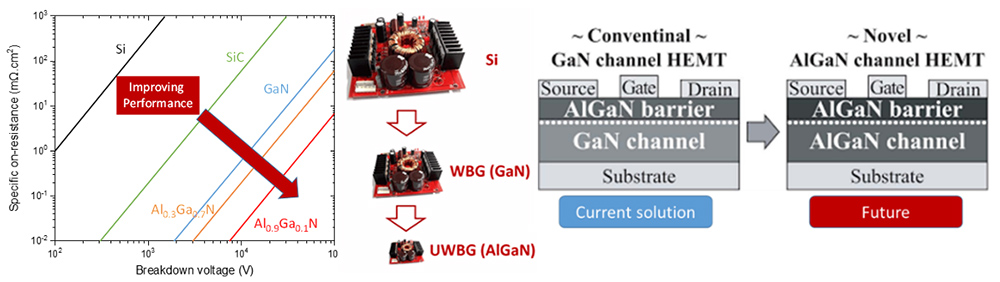
- The ACTION project aims to explore and develop a new breed of transistors using an ultra-wide bandgap AlGaN channel. This PRCE project is made up of three academic laboratories, CRHEA, IEMN and the Néel Institute, and the startup EasyGaN as the industrial partner.
- These AlGaN transistors will make it possible to lay the foundations for a future generation of power components that will offer higher operation voltage and temperature stability beyond the limits of GaN. The targeted performances will compete with contemporary SiC-based transistors. Thanks to the increased efficiency at high voltage operation (1200V), currently inaccessible to GaN-on-Silicon transistors, these components will reduce the losses that occur during the multiple transformations of electrical energy from its production to our daily use. The key point of the project is the development by molecular beam epitaxy (MBE) of AlGaN/AlGaN heterostructures on large diameter silicon substrates. These novel and CMOS compatible semiconductors will strengthen the current efforts of the main French players in the field. In the context of decarbonization and therefore a massive electrification, the ACTION project will play an important and strategic role in the creation of a new generation of semiconductor components improving energy management.
- This project is based on remarkable preliminary results since a breakdown field greater than 2.5 MV/cm has already been measured on extremely simple AlGaN channel HEMT structures. This breakdown field value is already beyond the state of the art of GaN-on-silicon HEMTs, which is typically around 1.5 MV/cm. These promising results confirm the interest of this approach, especially since these extremely simple structures (without strain engineering or defect density reduction) have been epitaxially grown on a silicon substrate. The ACTION project aims to develop AlGaN channel HEMT structures optimized in terms of defects and strain engineering on large diameter silicon substrates based on the unique CRHEA know-how of more than 20 years of MBE epitaxy. Part of this know-how has been already transferred to the startup EasyGaN. In particular, a patent which makes it possible to reduce the density of dislocations in the AlGaN alloy has been licensed to EasyGaN. Another key point of the ACTION project is the optimization of the different processing steps and the realization of the device. The team of Farid Medjdoub (IEMN) is at the state of the art in this field. Their expertise will make it possible to optimize the performance of the structures grown in the project. Julien Pernot's team (Institut Néel), recognized as a leader in the field of ultra-wide-gap materials, will provide an in-depth study of the properties of the AlGaN. In particular, the team will provide expertise on the electron transport properties which are the core of the project. All things considered, the ACTION project will enable EasyGaN to add a high value and strategic product to its catalogue.
- The partnership offers perfect complementarity by bringing unique know-how to carry out this ambitious project aimed at innovative power components. The project will also benefit from the expertise of external partners such as: - the company Knowmade specialized in patent analysis and consulting in technology watch and intellectual property strategy, - the University of Padua for dynamic measurements, - the University of Bristol for thermal analyzes and, - the SME Riber for developments and technical support around MBE growth on 8" substrates.
The main technological or characterization means that will be necessary to carry out the project:
- CNMF : Centrale de micro et nano fabrication
- Plateforme CHOP : caractérisation DC, pulsée, haute tension
Flagship projects concerned:
- Transportation
- Smart energy
- Micro-nano-devices
LABEX GANEXT
LABEX GANEXT :
Duration: 2020 – 2025
Coordinator of RF and power electronics: Farid Medjdoub
 Objectives:
GANEXT is a French national network including industrials and academics working on nitrides materials and devices.
A funding close to 4 M€ for 4 years has been granted by the ministry of research.
Main part of the activities are focusing on power and RF electronics. Funded projects aim at significantly supporting the roadmap of French industrials in this frame.
DGA/CNRS contract GREAT
DGA/CNRS contract GREAT :
High frequency GaN electronics
Duration: 2021 – 2025
Coordinator : Farid Medjdoub
As a strategic technology, GREAT has ben jointly funded by DGA and CNRS to improve millimeter-wave GaN transistors for future radar systems.
 Objectives:
•Develop a robust GaN technology (TRL 4) up to W-band
•Support the optimization of UMS next generation of GaN transistors (GH10)
•Understand the parasitic phenomena and related device degradation under high electric field of ultrashort GaN transistors
•Analytical physical modelling and simulation of devices and circuits
•Ka-band circuit design to validate benefit of the developed technology at the circuit level
Contract PEPR ELETRONIQUE VERTIGO
Contract PEPR ELETRONIQUE VERTIGO
VERTIcal Gan for high vOltage
Duration: 2022 – 2026
Coordinator : Cyril Buttay
Objectives
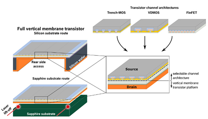
The proposed VERTIGO project aims to develop AlGaN nitride power transistors with a vertical geometry. Today’s technology for GaN power transistors is based on lateral HEMT where the voltage rise is obtained by increasing the space between the gate and the drain, to the detriment of the current and power density. In addition, these lateral-architecture components are necessarily sensitive to surface phenomena.The vertical geometry makes it possible to gain in current density, and the rise in voltage (the project targets 1200 V, with chips of a caliber of 50 A) is obtained with thicker layers. Finally, the increase in frequency is allowed by the important mobilities that the project will target by working on the conduction channel and exploiting all the possibilities offered by heterostructures. The project aims to reach a large increase (x10) in electronic mobility compared to current published results in the field.
Adequacy with the national Electronics plan:
VERTIGO aims to provide vertical power components in silicon GaN that offer the performance required by the industry, especially automotive. It relies on French research actors from the material to the system. In particular, the high voltage GaN is identified by automotive manufacturers as necessary to accompany the rise in voltage of on-board networks beyond 400 V (800 V targeted by several manufacturers), because it should make it possible to produce components at a lower cost than SiC technology.
Industrial project SmartGaN
The objective of this project is the study of vertical and lateral GaN power components produced on the so-called « SmartGaN for Power » substrate currently being developed at Soitec.
The principle of such a substrate is the transfer of a thin layer of monocrystalline GaN material (< 1 µm) onto a substrate called “base” via a bonding process. This bonding process may itself require a so-called “bonding layer” with electrical and thermal properties different from those of the base and the GaN layer.
PEPR GOTEN
OBJECTIVE
Pushing the limits of power electronics by means of Gallium oxide, the next generation power semiconductor
CHALLENGE
Demonstrate the viability of a French technology of vertical components based on gallium oxide (Ga2O3), covering the entire value chain ranging from epitaxial growth to thermal management of packaged components.
Completed Projects
EU ECSEL YesVGaN European Contract (Horizon 2020)
Contract EU ECSEL YesVGaN :
Vertical GaN on Silicon: Wide Band Gap Power at Silicon Cost
Duration: 2021 – 2025
Responsible for IEMN: Farid Medjdoub
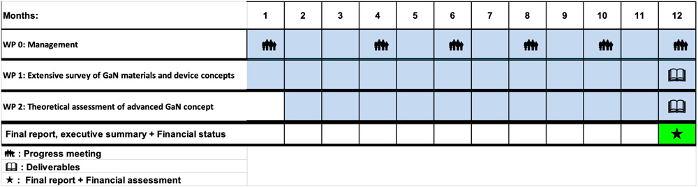
ESA European Contract (European Space Agency)
ESA European Contract (European Space Agency)
Duration: 2022
Coordinator : Farid Medjdoub
Objectives:
The proposed work aims to assess and quantify performances of new materials and device topologies of mmW GaN-based transistors allowing frequency extension up to W-band with the aim of achieving new stretch targets, especially in terms of ways to improve both power-added-efficiency and linearity. The novelty lies on an extensive survey of advanced concepts studied worldwide with respect to the whole figure of merits while including theoretical investigations of the most promising concepts based on TCAD simulations and checking the manufacturability of each approach with main EU epi-suppliers and foundries. The outputs from this study will allow ESA to focus its future GaN process development efforts to help enable a European supply chain for state of art mmW GaN MMIC technology.
Contract ANR DGA (ASTRID) CROCUS
Contract ANR DGA (ASTRID) CROCUS :
Circuits for robust Communication system in the millimeter wave range based on GaN-on-Si substrate
Duration: 2014 – 2017
Responsible for IEMN: Farid Medjdoub
Objectives:
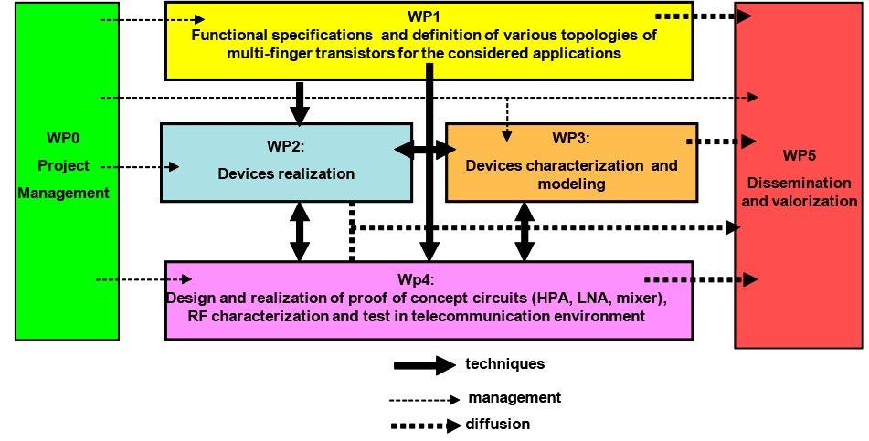
This project proposes to design, realize in hybrid integration and test some key Ka band circuits such as power amplifier (HPA), Low noise amplifier (LNA) and mixer, using EpiGaN epitaxies. These circuits will be developed with respect to Thales communication (military communication systems) and BLUWAN specifications (Civilian LMDS & Satellite applications).
Contract ANR DGA (ASTRID) COMPACT
Contract ANR DGA (ASTRID) COMPACT :
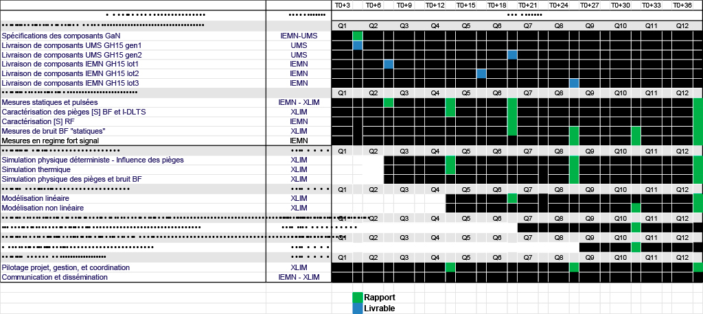
Understanding and optimization of trapping effects in the frame of the development of next generation of power devices for Ka band applications
Duration: 2018 – 2021
Responsible for IEMN: Farid Medjdoub
Objectives:
This project aims to solve inherent GaN technology issues related to electron trapping effects and thus optimizing key figures of merits such as power-added-efficiency and associated output power for transistors with sub-150 nm gate lengths.
Contract ANR LHOM
Contract ANR LHOM:
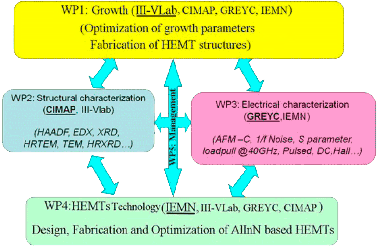
AlInN Layers and AlInN Heterostructures for Optimized high electron Mobility transistors
Duration: 2014 – 2017
Responsible for IEMN: Farid Medjdoub
Objectives:
The LHOM research effort establishes a strongly iterative methodology for sustaining the production of the next generation AlInN based high frequency high mobility electron transistors (HEMTs). In this project, three public institutions and a private company are to carry out an extensive investigation extending from the optimization of the growth of the layers and heterostructures to the fabrication and performance validation of the HEMTs for high power millimeter-wave range applications.
Contract ANR BREAkuP
Contract ANR BREAkuP:
Ultra-wide Bandgaps for futuRE high power electronic ApPlications
Duration: 2018 – 2021
Coordinator : Farid Medjdoub
Objectives:
To develop novel robust and reliable AlN-based power devices for high and medium power electronic systems targeting energy conversion efficiency as well as high frequency applications and bringing the Ultra-Wide-Bandgap semiconductors power devices another step towards the wide usability in the energy saving environment and next generation of millimeter-wave devices.
Contract FUI VeGaN
Contract FUI VeGaN:
Very Efficient GaN Amplifiers for Networks
Duration: 2015 – 2019
Responsible for IEMN: Farid Medjdoub
Objectives:
The aim of VeGaN is to contribute to the technology development for high frequency applications and enable the competitiveness of the critical GaN device EU industry, which is key for future telecommunication wireless systems.
Contract EU EDA (European Defense Agency) EUGANIC
Contract EU EDA (European Defense Agency) EUGANIC:
European GaN Integrated Circuits
Duration: 2016 – 2020
Responsible for IEMN: Farid Medjdoub
Objectives:
The main objective of the project is to close the European supply chain for military GaN-based electronics in order to secure the availability of GaN devices for strategic European defense projects. Therefore, European commercial suppliers of SiC substrates and state-of-the-art epitaxially grown wafers (epi-wafer) with HEMT (High Electron Mobility Transistor) layer structures suitable for microwave transistors and circuits shall be developed. With all these activities the project aims to create a leading-edge industrial supply chain for GaN-based electronics for the needs and applications of the European defense industry.
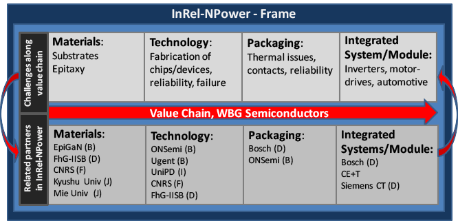
Contract EU H2020 Inrel-NPower
Contract EU H2020 Inrel-NPower:
Innovative Reliable Nitride based Power Devices and Applications
Duration: 2017 – 2020
Responsible for IEMN: Farid Medjdoub
The project has the following main objectives:
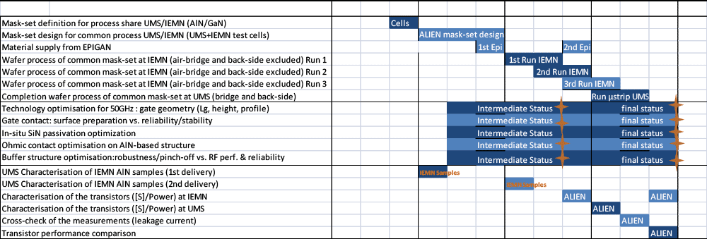
Industrial (UMS) bilateral contract ALIEN
Industrial (UMS) bilateral contract ALIEN:
Duration: 2018 – 2020
Responsible for IEMN: Farid Medjdoub
Objectives:
This project covers the evaluation of the AlN/GaN by developing a preindustrial process shared between IEMN and the foundry UMS on 4-inch SiC substrate including the uniformity, device size and reliability issues.