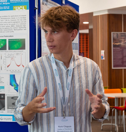
Rapidly interested in material science and nanoelectronics, Niels has carried out engineering studies at Polytech Grenoble, giving him fundamental knowledgeledges in microelectronics, surface characterization and semiconductors science.
In 2019, he joined the Master 2 programme in Material Science at the University of Tsukuba, Japan, specialized in nanoelectronics and semiconductors science. He was there introduced and trained on three devices development techniques: thin films growth by Molecular Beam Epitaxy (MBE) and Atomic Layer Deposition (ALD), and Inductive Coupled Plasma Reactive Ion Etching (ICP-RIE). This last technique lead to a master thesis project entitled "Comparative Study of Dry Etching of c-oriented Ga-polar GaN: ICP-RIE by Cl2/Ar and Cl2/Kr plasma" in which he used various characterization techniques (AFM, SEM, XPS, etc).
For his PhD thesis at the IEMN, Niels is focusing on the MBE growth of a WSe2/HfSe2 heterostructure on GaP(111)B substrate. The main goal of this project is to develop a type II p-n junction for tunnel diode. He is therefore focusing on crystalline and interface quality of epitaxial layers, performing thorough morphologic, crystallographic and electronic properties characterizations.


