

T1 : Science des matériaux organiques et nanotechnologie moléculaires
Cette thématique plus fondamentale porte sur la fabrication de structures, la caractérisation des structures et des propriétés de transport électronique ou thermique.
Les aspects explorés dans cette thématique sont par exemple :
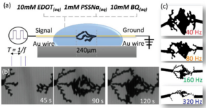
- L’étude de la croissance de dendrites électropolymérisées [SciRep22]
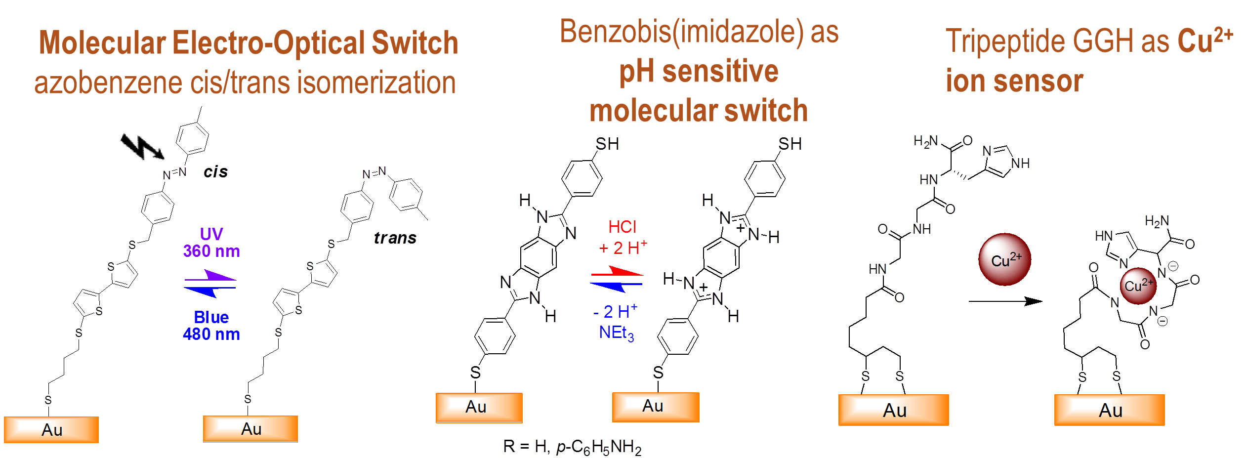
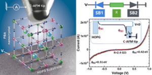
- Le transport électronique à l’échelle du nanomètre mesuré par Conductive-AFM sur les polyoxometalate [Nanoscale18; Nanoscale22] ou sur des nanocristaux de Co et Ni analogues de bleu de Prusse [Nanoscale20 ; Nanoscale23) ou encore sur des interrupteurs moléculaires déposés en monocouche auto-assemblée comme les dérivés azobenzènes [Nanoscale21] ou diaryléthènes [Nanoscale22)
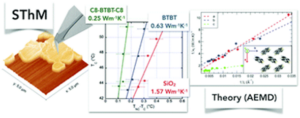
- Les propriétés thermiques en fonction de la structure des molécules organiques considérées (différents substituants, présence de métaux de transition) sont également étudiées à l’aide du Scanning Thermal Microscope [Nanoscale21; Nanoscale22].
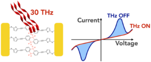
- La démonstration de photocommutateurs terahertz mesurés par Conductive-AFM et à base de monocouches moléculaires auto-assemblées (SAM). [Nanoscale24]
T2 : Dispositifs et calculs neuromorphiques à base de matériaux organiques
Chemical synthesis