Clément BARBOT
PhD student « Epitaxial growth and near-field characterization of InSb nanostructures for advanced electron devices »
+33 (0)3 20 19 78 65
clement.barbot@univ-lille.fr
Graduated in 2019 from a material science engineering degree at EEIGM (Ecole Européenne d’Ingénieur en Génie des Matériaux) in Nancy, he studied there all classes of materials in details (glass, wood, ceramics, semiconductors, metals, and so on…). As part of the program, courses about quantum physics and semiconductors properties were attended as well. Additionally, an international exchange program he took part at the LTU (Lulea Tekniska Universitet) in Sweden, 2018, offered him the possibility to further study the material characterization techniques (SEM/TEM, STM; AFM, PL, Raman, XRD, etc…).
The various work experience he gained so far (see below) allowed him to build a strong interest, extensive knowledge on the nanotechnology field and to develop a first good hands-on practice with advanced equipments:
- 6 months lab internship at the IJL (Institut Jean Lamour) in Nancy on ZnO layer optimization via RF sputtering (PVD)
- 6 months industrial internship at the CRM (Centre de Recherche en Métallurgie) in Liège (Belgium) on Alkali Doping (Na,K) of CuInGaSe solar cells
- Dec 2019 to July 2022 at IMEC Leuven (Belgium) as a Process Engineer within the in-Line Metrology Team (Inbspection, XRD, Ellipsometry, SEM, Sheetresistance, Chemical Contam ToF-SIMS, etc…), daily work in 200&300mm Si cleanrooms
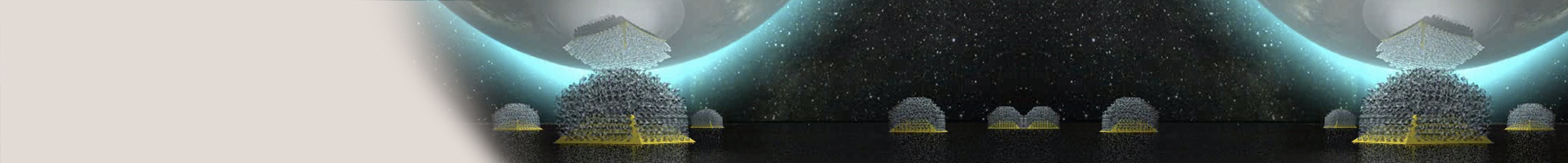
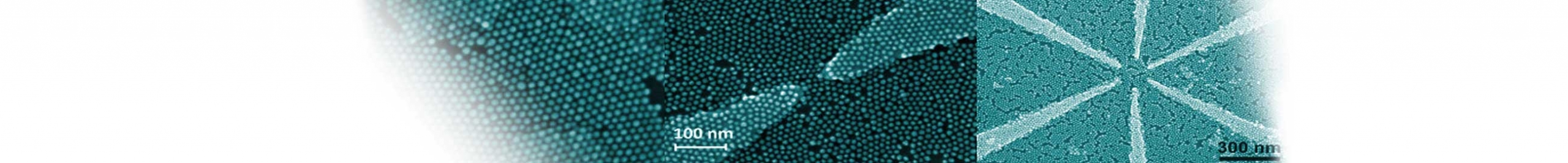
During his time at IEMN, he will be interested in the SAG (Selective Area Growth) of InSb nanowires via MBE technique on various substrates (GaAs, GaInP, CdTe) and their physical characterization via AFM,STM and Nanoprobe (4PP measurement) in the perspective of evidencing enhanced electronic-transport in such devices.


