Graphene growth
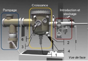 Located in a stat-of-the-art clean room, our equipment enables:
- Graphitization on silicium
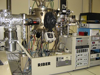
- Molecular beam epitaxy on silicium, an exclusive technology that enables to control graphene layer’s thickness
- CVD growth on metals (Cu, Ni)
Carbon has also developed state-of-the art techniques to transfer graphene from catalyst to different substrates.
Graphene nano-devices
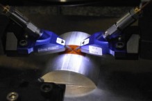 Our team can design, develop and characterize a wide range of graphene nano-devices to match various potential industrial applications: Nanoribbon FET on SiC, RF characterization, transfer on materials, flexible supports, etc.
Our technology platform include three molecular beam epitaxy (MBE) chambers, dedicated to III-V material and graphene growth, and are coupled together with the ESCA analysis chamber under ultra-high-vacuum.
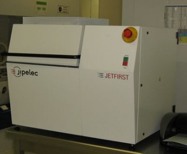
Two chemical vapor deposition systems enable the growth of Si and Ge nano-wires and graphene growth on metals.
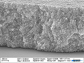
Characterization tools provide structural (X-ray diffractometer, atomic force microscope and scanning electron microscope), surface (ESCA), electrical (Hall effect), optical (photoluminescence, micro-photoluminescence), thermogravimetry and mass spectroscopy in-depth analysis.
Ink-jet technology
Carbon Research Group has pioneered the use of inkjet printing within the frame of nanotechnology-related projects.
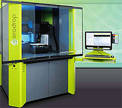
Our teams relies on CERADROP inkjet printing equipment and is able to build elaborate nano devices.
Carbon benefits from a unique know-how in pattern design simulation, temperature treatments, inks and substrates formulation and optimization (nanoparticle grain size analysis, ink rheology, surface tension and drying, thermal treatment of materials).
This know-how enables our team to work on flexible devices and transistors and to use a broad range of materials for manufacturing novel devices: plastic electronics, flexible displays and biosensors.
Tests performed by industrial partners proved out manufacturing techniques for flexible electronics both performant and robust.


