

hen the dimensions of materials reach the nanometer scale, the objects have fascinating properties, mainly related to principles of quantum mechanics. Our main goal is too deepen our understanding of these properties. Our team belongs to IEMN, one of the few national laboratories with state of the art facilities that allow us to develop processes and applications of nano-scale materials, structure and devices. We are also strongly involved in the development of instruments that are appropriate to probe the matter at the nanometer scale, such as scanning probe microscopies. Although we perform fundamental studies, our research activities include pratical applications in the fields of solar cells, neuromorphic devices and quantum information processing.
Nanofabrication
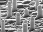 Both defining and positioning structures with sub-10 nm accuracy is beyond the limits of conventional lithographic techniques. In contrast, natural interactions between atoms and molecules produce kinetically and thermodynamically preferred structures and patterns. Our challenge consists in controlling the spontaneous formation of crystalline structures at the nanometer scale. These nanotructures are either metallic or semiconductor and can be made up of organic or inorganic materials. For example, we grow nanowires using metal nanoparticles as catalysts (see upper figure) and also synthesize quantum dots or produce ultra thin films, that may require multidisciplinary knowledges gained from collaborations with other research laboratories that are mainly based in Lille.
Electronic and vibrational excitation of nanoscale objects
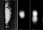 When the dimensions of semiconductor materials reach the nanometer scale, quantum mechanics have a substantial impact on their properties. Tailoring these properties offers a vast number of new possibilities in nanodevice technology. There is thus a critical need for the growth and the characterization of low dimensional semiconductor systems. Many of our studies rely on the use of scanning probe microscopies, since these tools enable both the direct observation of individual semiconductor objects with reduced sizes and the characterization of their electronic structure as well as their transport and charging properties. As an example, the left image in the upper figure shows a (110) surface obtained with a scanning tunneling microscope where a cleaved InAs quantum dot embedded in GaAs materials is visible at the atomic resolution. By probing the electronic structure of the dot at low temperature, conductance maps corresponding to the square of the electron wave function can be obtained at the energy of the ground (middle) and first excited (right) states.
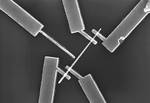 We also work on integrating these nanostructures in devices, as building block for quantum computing for example. In these configurations, the study of transport through the nanostructures allows to gain insight into quantum coherence, correlation effects and noise. The SEM image to the right shows a Si nanowire, grown by chemical vapor deposition and transferred to a silicon oxyde layer, where it has been connected to electrodes.
Advanced technology
 We continously work to develop new measurement methods and tools related to scanning probe microscopies, with capabilities beyond the commercial state of the art. All the systems are part of the iemn Excelsior facility, that host high frequency characterization tools, from DC to THz, and a large variety of scanning probe microscopes.


