GaN and nitride-based wide gap materials are extremely promising for the realization of both high frequency and high power electronic devices. Some theoretical investigations have been performed in this context.
1. In the framework of the ANR project SATELLITE (coordinator JC De Jaeger, head of PUISSANCE group), we developed Monte Carlo tools for studying electron transport in bulk nitride materials, heterostructures and HEMTs devices. As a byproduct of this work, we obtained transport parameters for these materials directly usable in device macroscopic modeling.
2. The potential of vertical GaN transferred electron devices (TED) for the realization of RF power sources at THz frequencies has been evaluated by means of time-domain quasi-electrostatic modeling associated to energy-momentum macroscopic approach for the free electron transport modeling.
Their RF properties fundamentally rely on the velocity-field characteristics of GaN exhibiting high mobility, large peak velocity and negative differential mobility. Theoretical investigations tend to demonstrate that mesa GaN TEDs operating in the accumulation layer transit time mode can be a candidate for the realization of RF low-power sources at 1 THz. However, this frequency must be considered as close to the maximum achievable one because of the limitation resulting from the device low negative resistance. The oscillator net performance will be dependent on the quality of the RF load circuit in terms of impedance matching capabilities and RF loss level. Moreover, the thermal limitation must be also considered. In fact, because of the required high DC bias conditions, only a strongly cooled CW or a pulsed RF operation seems achievable.
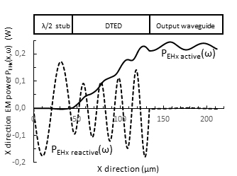
3. A more prospective study is devoted to THz GaN planar distributed TEDs. Their RF operation is based on the interaction between an electromagnetic wave propagating in a plane parallel to the device epitaxial layers and electron moving perpendicularly under the accumulation layer and transit mode. Thus, the device active zone behaves as a negative resistance medium leading to the electromagnetic wave amplitude amplification. The device non-linear and complex RF operation is studied by means of a physical time-domain electromagnetic/macroscopic transport model. The potential of THz full planar waveguide based oscillators is presently investigated. The expected DTED RF operation based on the amplification of a quasi-transverse electromagnetic wave has been confirmed.
The modeling is now extended to the whole oscillator including the circuit elements constituting the external load circuit in order to account for and consequently optimize the active device/ load circuit energy transfer.
Another DTED oscillator structure based on the planar waveguide/ output plasmonic waveguide technology is also under investigation.


