The SPM facility brings together resources dedicated to the topographical, physical and electrical analysis of surfaces down tothe atomic scale..
 This direct investigation technique at the nanometric scale is at the origin of the emergence of nanosciences and nanotechnologies. As soon as it was created in 1993, theIEMN has decided to acquire this imaging equipment, manipulate and characterise nanometric atoms and objects. The SPM facility is housed in a 400m2 dedicated building, completed in 2015, offering exceptional experimental conditions.
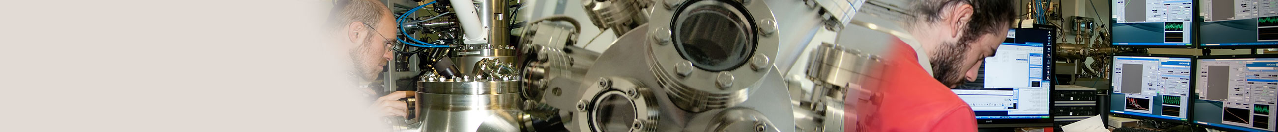
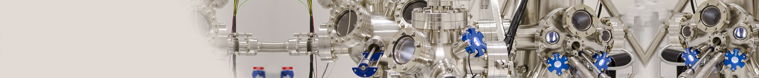
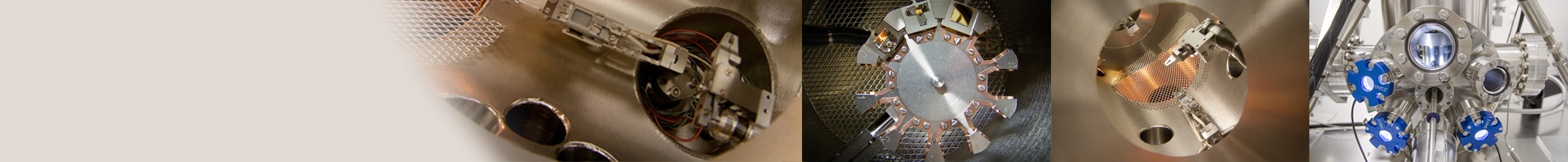
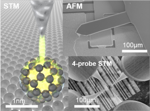
Our instruments cover a broad spectrum of possibilities for the direct measurement of phenomena at the nanometric scale : AFM in air and derived modes, AFM/STM in ultra-high vacuum, nano-manipulation, (multi-tip) measurements of transport at the nanometric scale, and a combination of SEM/STM/AFM. The near-field microscopy centre is dedicated to supporting the IEMN's research activities; it is also open to any external request for services or collaboration, academic or industrial, via RENATECH network..

UHV domain
Air Domain
Contact: Maxime BERTHE, Responsable du pôle
maxime.bertheuniv-lille.fr 03 20 19 79 79
Keywords: 3D microscopy, SPM, STM, AFM, Sub-nanometer resolution, Physical nanocharacterization, Renatech
Application areas: Nanoscience, Physics of surfaces, materials and nanostructures, Surface chemistry
Download the brochure (version 4 sept. 2024)


