![]()
Réalisations
Nous disposons d’ateliers d’électronique sur les pôles SigmaCom et C2EM, dotés d’équipements de prototypage rapide pour produire des circuits imprimés.
Moyens présents sur le pôle C2EM :
• Autodesk Eagle and Fusion 360
Schematic with Electrical Rule Check
Board with Design Rule Check
ECAD-MCAD co-design process
• LPKF PCB milling machine ProtoMat S63
Mat. Size 229x305mm
Resolution 0.5µm
Automatic tool change
Minimum isolation 0.15mm
Minimum width 0.15mm
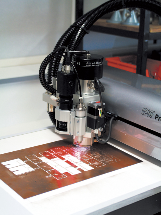
• LPKF ProtoLaser H4
Mat. Size 305x229x7mm
Résolution 1µm
Automatic tool change for drilling
Minimum isolation 30µm
Minimum width 50µm (tested)
• LPKF Multipress-II (multi-Layer) – Up to 6 layers
• LPKF MiniContact RS – Holes Metallization
Max. material size (X x Y) 230 mm x 330 mm (9” x 13”)
Max. layout area (X x Y) 200 mm x 300 mm (7.8” x 11.8”)
Reverse pulse plating Adjustable
Tolerance ± 2 μm (0.08 Mil), copper coating
Minimum hole diameter ≥ 0.2 mm (8 mil)
ViaCleaner Included
Chemical tinning Included
• Tools for component assembly and welding

ProtoLaser H4 – système hybride de gravure laser LPKF
Moyens présents sur le pôle SigmaCom :
• PCB Design Package TINA
• LPKF PCB ProtoMat H100 fully Automated
Mat. Size 400×360 mm – Resolution 0.25μm – Minimum isolation 0.1mm – Minimum width 0.1mm – Minimum hole diameter 0.15 mm – Automatic 30 position tool changer – Optical fiducial recognition
• Semi-automatic station for SMD assembly
• SMD soldering by reflow furnace
Mechanical engraver for the realization of high frequency circuit boards


