NANO CHARACTERIZATION
_________
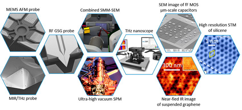
IEMN is a key player in advanced nanoscale measurement science. This is due to a unique, cutting-edge ecosystem gathering scanning probe and RF know-how, and research groups addressing a wide range of nanotechnology topics spanning fundamental molecular nanoscience to RF nanodevices. Nanocharacterization is a transverse topic at IEMN— it is widely used in research groups and links two established technological facilities, and also since IEMN projects are clearly oriented towards the development of unique nanocharacterization capabilities.
One motivation of the project is to tackle the issues between spatial resolution and frequency domain by combining scanning probe microscopy techniques and broadband spectroscopy tools, already broached within the PIA Excelsior project. Another aim is to use such advanced nanotechnology tools to address interdisciplinary topics in the fields of nanostructures or molecular devices, sensors and biosensors, energy and environmental issues. By such developments, the research groups and technology platforms of IEMN aim to accelerate fundamental research in nanoscience and innovation in nanotechnology-based industry, by establishing partnerships and collaboration with academic, metrology and industrial laboratories, and by promoting innovation and industrial competitiveness, both at national and international levels.
Objectives
Development of techniques for the morphological/electrical/magnetic/thermal/mechanical/chemical characterization and quantitative measurements of innovative/smart/active nanomaterials, nanodevices and nanosystems beyond the state-of-the art. For this purpose, we combine scientific investigations together with hardware instrument developments based on IEMN expertise in nanoscience, electrical engineering, micro/nanofabrication technologies.
Key challenge 1: Simultaneous microscopy and spectroscopy in a wide frequency spectrum.
Microscopy tools are based on micro/nanomanipulation, atomic force / scanning tunnelling microscopy (AFM, STM), scanning electron microscopy (SEM), scanning microwave microscopy (SMM), optical (THz) trapping, coupled with spectroscopy equipment such as RF, GHz to THz, IR to visible light sources and sensors (including ultra low-noise and ultimately quantum sources and sensors). Scientific objectives will consist in e.g. characterizing local electronic devices with spatial resolution in the 1-10 nm range beyond 40 GHz (SMM); characterizing emerging nanomaterials and devices for photovoltaics (such as perovskites) with either combined temporal (sub-ps) /spatial resolution (sub-nm) with STM or AFM.
Key challenge 2: Advanced probes based on micro and nanotechnologies.
Combined micro and nanotechnologies can make a major contribution to scanning probe microscopies, for instance by enabling the control of metallic features forming an original/optimized micro/nanofabricated probe, or designing specific substrate geometries. Recent achievements and on-going projects at IEMN are e.g. miniaturized ground-signal-ground probes for on-chip microwave measurements (Excelsior); metasurfaces for local THz spectroscopy; high-frequency atomic force microscopy probes (PIA Vibbnano, ANR emergence vibrations, industry transfer to Vmicro); and prototypes of tip enhanced Raman spectroscopy (TERS) probes (joint lab. with HORIBA France). The quest for advanced probes will also include spectroscopy instrumentation integrated in the probe environment for RF measurements (joint IEMN–ST Microelectronics lab). Such developments will give unique performances to the IEMN measurement tools at the forefront of researches involving nanoscale characterizations, with fallouts as spin-off creations.
Key challenge 3: Addressing scientific and instrumental issues in controlled environments (vacuum, temperature, liquid).
New instrumentation fields are required to address upcoming scientific challenges. For instance, research for quantum computing and communications will require microwave microscopy, or microwave STM/AFM under magnetic field at low temperature. Alternatively, biology faces the issues of high speed and in-depth imaging of living cells in liquid media, while biosensing (e.g. sensors, use of chemically patterned substrates) or the development of materials related with energy (e.g. microbatteries) will require combined mechanical or electrical measurements in liquids. It will the aim of this challenge to develop measurements in such controlled environments. One particular issue will lay in obtaining quantitative or calibrated measurements towards nanometrology standards, in link with metrology labs (LNE, METAS, VSL, NPL, PTB) at the EU level and the NIST in US.
Coordinators:
Contact : kamel.haddadi ![]() iemn.fr
iemn.fr
Contact : maxime.berthe ![]() iemn.fr
iemn.fr
