MATERIALS
_____________________
The Materials Flagship of the IEMN gathers all the activities related to materials: elaboration, characterization, structuring and simulation. It is a transverse Flagship that works in close collaboration with the two other transverse Flagships: 'Nanocaracterization' and 'Micro and nano devices'. The developments carried out enable the Institute's thematic Flagships to be fed, such as 'Smart Energy', 'Ultra High Speed Telecommunications', 'Neuromorphic Technologies' and 'Technologies for Health'.
The Materials Flagship of the IEMN gathers all the activities related to materials: elaboration, characterization, structuring and simulation. It is a transverse Flagship that works in close collaboration with the two other transverse Flagships: 'Nanocaracterization' and 'Micro and nano devices'. The developments carried out enable the Institute's thematic Flagships to be fed, such as 'Smart Energy', 'Ultra High Speed Telecommunications', 'Neuromorphic Technologies' and 'Technologies for Health'.
Historically focused on III-V semiconductor materials for high-frequency microelectronics and optoelectronics, IEMN's materials activity has diversified considerably to satisfy new scientific themes. The semiconductor field has been extended to silicon and functional materials for micro and nanoelectronics, MEMS, sensors and microsystems. The interface with other scientific fields has opened up new avenues of research in organic materials for the development of specific electronics or the functionalization of surfaces. Two-dimensional materials, based on carbon in particular, have also been the subject of increasing activity within the IEMN. Finally, this flagship includes artificial materials defined as composite structures under wavelength (metamaterials, metasurfaces).
The Flagship materials aims to federate the strengths of the Institute and to promote synergies between the various actors according to the following objectives:
- Ensure the sustainable development of established materials
- Study the synthesis of new materials or combinations of materials
- Structuring materials under wavelength
- Functionalize surfaces
- Simulate and model material properties
- Develop new and more sustainable technological processes
- Microwave and THz microelectronics
- Intelligent sensors for environmental control
- Energy storage
- Metamaterials for wave control, from acoustic to infrared
- Organic electronics
- Precision health
- Quantum technologies
Synthesis of materials
Seven families of materials are developed (semiconductors, dielectrics, metals, functional materials, organic materials, nitrides and 2D materials), each family having its preferred manufacturing techniques.
III-Vs semiconductors (arsenides, phosphides and antimonides) are epitaxialized by molecular beam epitaxy (MBE) while low pressure chemical vapor deposition (LPCVD) is used for polysilicon. Liquid phase synthesis is used to fabricate arrays of organized nanocrystals.
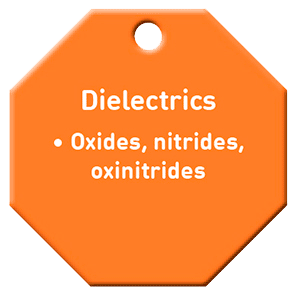
CVD and its variants (plasma assisted CVD) as well as atomic layer deposition (ALD) are the main techniques for dielectric synthesis (SiO2, SixNy, TiOx, Al2O3, HfO2).
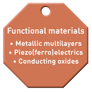
The functional materials and their heterostructures as well as the nitrides are obtained mainly by sputtering but also by hydrothermal method.
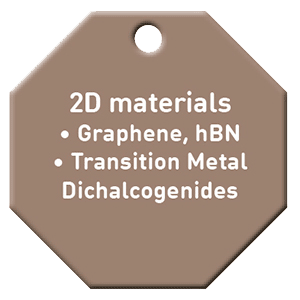
Some 2D materials (graphene, hBN, TMDCs) are epitaxial by EJM or CVD but the exfoliation of bulk samples allows to extend the range of available materials and to work on sheets.
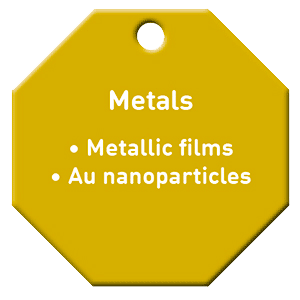
The metallic deposits use different techniques, evaporation by Joule effect or by electron gun, sputtering, ALD, depending on the nature of the metal and the thickness considered.
The synthesis of organic materials also involves different technologies: spinning deposition, sol-gel process, physical vapor deposition (PVD) and chemical synthesis.
Characterization of materials
The numerous equipments available in the Micro and Nano Manufacturing Center but also in the Multi Physics Characterization Platform allow to obtain a complementary characterization of materials at different scales.
Profilometry, optical and scanning electron microscopy, atomic force microscopy and tunneling microscopy are the key tools for the determination of sample morphology.
Optical properties are probed by ellipsometry, Raman spectroscopy and µ-photoluminescence.
The physicochemistry of the samples is studied by EDX analysis while that of the surfaces and interfaces is determined by X-ray and UV photoelectron spectroscopy. Tunneling spectroscopy gives access to surface electronic properties with ultimate resolution.
The crystallography of the synthesized materials can be studied by electron backscatter diffraction (EBSD) and X-ray diffraction.
We also have the Wavesurf platform which exploits the dispersion of surface acoustic waves and uses guided probes and a picoacoustic device to determine the dimensional characteristics of layers and their elastic and mechanical constants. Magnetic properties are obtained by magnetometry.
The electrical properties are deduced from measurements of non-contact resistivity, Hall effect and I(V) characteristics taken on different dedicated benches.
Modeling and simulation
Transport properties in 2D and 3D semiconductors and polarization properties in ferroelectric materials are studied by Monte Carlo method.
The simulation of sub-wavelength structures (acoustic and electromagnetic metamaterials and metasurfaces) is performed by the finite element method in the frequency domain or finite differences in the time domain.
The micro instabilities/bistabilities of materials are studied by statistical mechanics.
The electronic structure of materials is calculated by ab initio (DFT) and empirical methods
Coordinators:
Contact : xavier.wallart ![]() iemn.fr
iemn.fr
Contact : Nicolas. tiercelin ![]() iemn.fr
iemn.fr
Contact : eric.lheurette ![]() univ-lille.fr
univ-lille.fr


