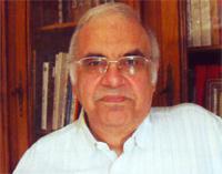
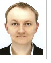
An IEMN researcher is awarded an ERC Starting Grant !

The project, named UPTEG « Unconventional Principles of ThermoElectric Generation », propose to test two unorthodox ideas to turn silicon into a thermoelectric material ! Indeed, thermal to electric energy conversion via Seebeck effect remains an inefficient process especially for low temperature gradients. In addition, conventional thermoelectric materials are polluting, rare and hardly compatible with microelectronics mainstream technologies…
However, silicon, which is a key material of microelectronics thanks to its electric propoerties, has an important Seebeck coefficient but suffers from a high thermal conductivity…

The project proposed by Jean-François Robillard, associate-professor at l’ISEN (Institut Supérieur d’Electronique et du Numérique) and researcher in the IEMN Microelectronics group rely on two approaches :
Phononic Engineering Converters : This approach envisions the periodic nanopatterning of silicon at the scale of the thermal phonon mean free path. This « artificial material » will exhibit a reduced thermal conductivity, down to 100 fold or 1000 fold as compared to bulk, and preserved electric properties.
Micro-Thermionic Converters : This approach is even more unorthodox and relies on building silicon electrode pairs separated by a vacuum gap in order to nearly supress thermal losses. The electrodes are functionalized thanks to low-workfunction material coatings (alcali oxydes) which enable electronic thermo-emission.
This research could lead to a better understanding of nanoscale heat transport and enable the fabrication of efficient micro-generators. Future developments envision mechanically flexible converters able to fit any surface.
The project relies on an ambitious program from simulation and material engineering to technology. It will benefit from the outstanding micro and nanofabrication facilities and caracterisation tools of the IEMN.
The European Research Council will provide funding up to 1.5 million Euros over the 5 years of the project which will lead to the recruitment of 5 PhD students and research associates, technological developments and dissemination activities toward general public as well as the scientific community.

Visite du Pr. François BOONE de l’Université de Sherbrooke au Canada

This invitation is part of an international research and training partnership between the Universities of Science and Technology of Lille 1 and Sherbrooke in Canada. The laboratories involved are the Centre de Recherches en Nanofabrication et en Nanocaractérisation (CRN2) at the University of Sherbrooke (Canada) and the Institute of Electronics, Microelectronics and Nanotechnology (IEMN) at the University of Lille 1. This operation is part of the UMI CNRS 3463: Nanotechnologies and Nanosystems Laboratory (LN2), which was created in July 2012 to maximise the international impact of research work in North America.

The aim is to design and manufacture components and circuits based on gallium arsenide, using the complementary expertise and resources of the two laboratories. Current activities, which began in September 2012 or are planned, concern several areas:

- Design of circuits with a view to their manufacture. The aim is to set up models relating to active and passive elements with a view to being able to design MMIC-type circuits.

- Production of MMIC circuits based on HEMT AlGaN/GaN and InAIN/GaN components for microwave power applications at 94GHz.

- Production of MMIC circuits based on HEMT AlGaN/GaN and InAIN/GaN components for power electronics applications.

This activity benefits from a doctoral student under joint supervision between the two laboratories: Adrien CUTIVET, who began his thesis work on 1 January 2008.er September 2012 as part of a co-funding agreement between the University of Sherbrooke and the President of the University of Lille1. The thesis co-supervisors are Prof. François BOONE, who is the subject of this invitation, and Prof. Jean-Claude De JAEGER. The purpose of F. BOONE's visit is to work directly with the IEMN researchers and A. CUTIVET in order to set up models of passive and active elements to establish a design kit dedicated to the design of Gallium Nitride Monolithic Integrated Circuits for microwave power amplification in the Ka, V and W bands.


Contact: Jean-Claude De JAEGER

IEMN involved in the Graphène project, winner of the European "FET Flagship" programme

Retenu par la Commission Européenne comme un des projets phare, d’une ampleur sans précédent, sur les technologies du futur et émergentes, le projet Graphène, financé à hauteur de 1 milliard d’euros sur 10 ans, mobilise 15 laboratoires Français, parmi lesquels l’IEMN.

Le projet Graphène vise à développer les applications d’un matériau constitué d’une feuille de carbone dont l’épaisseur est réduite à une seule couche d’atomes : ses propriétés mécaniques et électriques exceptionnelles lui ouvrent des applications dans tous les domaines, de la microélectronique aux pièces aéronautiques. Il rassemble 126 équipes de recherche de 17 pays.

Lire le communiqué de presse


Contact:
Professeur Henri HAPPY
Tel: +33 (0)3 20 19 78 41 Fax: +33 (0)3 20 19 78 92
Courriel: henri.happy@iemn.univ-lille1.fr

IEMN is recruiting

Un Responsable des moyens « back-end » des plateformes de l’institut.

Le responsable aura la charge de l’intégration des composants dans des systèmes et de mise en boîtiers de la découpe, amincissement de wafers.

 Context :
L’IEMN est un laboratoire de recherche de 500 personnes qui joue un rôle majeur au niveau international dans le domaine de la recherche en microélectronique et nanotechnologie. Pour cela, les différentes équipes de recherche de l’institut s’appuient sur quatre plateformes technologiques de haut niveau dont la centrale de micro et nano technologies (1 600 m²).
Le poste est un support technique participant au développement et à la réalisation de systèmes électroniques qui se développe au sein des plateformes techniques et plus particulièrement dans le cadre des projets Equipex « Excelsior » et « Leaf ».

Read more

Kick-off Meeting RTB Network

Un réseau, à disposition de tous ceux qui ont besoin de réaliser des micro ou nano objets vous invite à une journée d’information et d’échanges pour vous informer sur les possibilités d’accès aux ressources technologiques du réseau de recherches technologiques de base (RTB),

le Vendredi 29 mars 2013, de 10h à 16h au Laboratoire Central de l’IEMN à Villeneuve d’Ascq.

Venez :

  • DECOUVRIR or REVOIR nos centrales de technologie,
  • INITIER une collaboration scientifique ou technologique,
  • EVALUER si l’accès à nos centrales peut vous intéresser

La journée annuelle des utilisateurs (actuels ou futurs) du réseau RTB est un rendez-vous national de l’ensemble des communautés académiques et industrielles (PME, Start-up, Grands Groupes) intéressées par les micro- et nanotechnologies. Grâce au soutien de l’ANR, ce réseau présente aujourd’hui un ensemble d’équipements et de savoir-faire au meilleur niveau international

 Cette journée est une opportunité pour :

  • VISITER une des centrales du réseau
  • APPROCHER le monde des nanosciences
  • DECOUVRIR nos réalisations obtenues en partenariat avec des académiques, des PME, des start-up, des industriels, …
  • CONNAITRE nos conditions d’accès, nos formations, …
  • ECHANGER sur vos projets et savoir si nous pourrions vous aider à transformer votre idée en composant ou dispositif.

La matinée sera consacrée à une présentation du réseau national des grandes centrales (RENATECH CNRS et CEA-Leti) et des projets technologiques phares réalisés récemment en partenariat scientifique ou industriel. Nos « utilisateurs » actuels vous feront part de leur expérience du réseau et des résultats obtenus. Les moyens et compétences technologiques du réseau ainsi que ses modalités d’accès seront détaillés.

L’après-midi sera consacré à une visite des installations et à des discussions/débats.Vous pourrez rencontrer nos chercheurs, ingénieurs et techniciens, ainsi que les responsables de l’accueil des projets d’utilisateurs extérieurs.

Modalités d’inscription (inscription gratuite) :

Pour vous inscrire, merci de renvoyer avant le 15 mars les informations ci-dessous par courriel à la centrale technologique de votre choix :

1. Nom, Prénom, Organisme/Entreprise, Adresse complète

2. Domaine/Thématique d’intérêt (ex. photonique,électronique, etc.)

3. Participera (i) au déjeuner (ii) à la visite de la salle blanche (OUI/NON)

Une confirmation d’inscription vous sera retournée avec le programme détaillé et les modalités d’accès.

Contact:

– A Lille, contacter l’IEMN (plateforme@iemn.univ-lille1.fr)

– En Ile de France, les centrales de l’IEF et du LPN seront présentées sur le site de Marcoussis (Anne.Talneau@lpn.cnrs.fr)

– A Besançon, contacter FEMTO-ST (servicecommunication@femto-st.fr)

– A Grenoble, contacter soit le LTM / CNRS (thierry.chevolleau@cea.fr), soit le LETI / CEA (thierry.billon@cea.fr)

– A Toulouse, contacter le LAAS (mplana@laas.fr)

Sites web :


Equipex LEAF Project

Equipex LEAF Project : ‘Laser procEssing plAtform for multiFunctional electronics on Flex’

Kick-off Meeting

20th Wednesday of March 2013

IEMN, Avenue Poincaré, Villeneuve d’Ascq, France

Open on morning (registration required)

AGENDA

9:30                     Welcome and Registration  (IEMN Hall)

10:00 – 10h30     Presentation EQUIPEX LEAF project

10:30 – 11:10       Daniel BENSAHEL ( Manager advanced front-end materials) ST Microelectronics, Crolles

« CMOS technology evolutions and new materials challenges »

11:10 – 11:50        Jan ELIZALDE (Senior Research Scientist) CIC microGUNE / IK4-Ikerlan, Arrasate-Mondragón

« Pathogens rapid detection Point Of Care (POC) for food contamination monitoring »

12:30 – 13:45       Lunch ( Basement)

13:45 – 14:30       Visit of IEMN  technological platforms

14:30 – 16:00        Executive and Steering Comittees

16:00                     End of kick-off meeting


LEAF-Web-Invitation-Kick-Off-final


On-line free registration: http://leaf-equipex.iemn.univ-lille1.fr/2013/01/24/kick-off-meeting/


Kick-off Meeting RTB Network

29/03/2013 –  10:00 (am)  to 04:00 (pm)

The network to basic research of technology (RTB), is a national network to large platform of micro- and nanofabrication.

Ce réseau est à disposition de l’ensemble des communautés académiques et industrielles intéressées par les micro et nanotechnologies et vous invite à une journée d’informations et d’échanges sur les possibilités d’accès à ces ressources technologiques le Vendrdi 29 mars 2013, de 10h à 16h à l’IEMN. Vous trouverez ci joint un descriptif de la journée . Registration required before 15th of March

Contact: plateforme@iemn.univ-lille1.fr

Detailed program of the day

SEMINAR Nano-FTIR: infrared spectroscopic chemical identification of materials at nanoscale

SEMINAR POSTPONE IN MARCH

 
- The NeaSNOM Microscope

- Nano-FTIR: Infrared spectroscopic chemical identification of materials at nanoscale".
by Dr. Andreas HUBER from Neaspec GmbH

February 6th; 14:30 Council room

 ‘Transport experiments in graphene devices, from exfoliated to epitaxial graphene’
par Dr Emiliano Pallecchi; Laboratoire de Photonique et de Nanostructures, Marcoussy

Key words: Cooling of hot electrons in graphene; GHz Jonshon noise thermometry; electron-acoustic phonons scattering;
supercollisions,  experiments on devices based on epitaxial graphene; magneto-transport experiments; ARPES measurements;
oxygen adsorption on the electronics properties.

www.excelsior-ncc.eu

Job opportunities

A lecturer/researcher - EMC and telecommunications and a lecturer/researcher - high-performance electronics using 2D materials

-> More details...