Séminaire : Simultaneous Information and Energy Transmission »
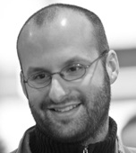
 Samir M. PERLAZA
Chargé de Recherche à l’INRIA
Visiting Research Scholar at Princeton University, NJ, USA
Editor of the IEEE Trans. on Communications
Editor of the IET on Smart Grids
jeudi 4 octobre 2019 à 14h00 – salle du conseil de l’IRCICA
Abstract:
In this talk, a review of recent advancements on simultaneous information and energy transmission (SIET) is presented. More specifically, SIET refers to communication systems in which a set of transmitters aim to simultaneously carry on two tasks: information transmission to a set of information receivers (IRs); and energy transmission to a set of energy harvesters (EHs). The performance of SIET is often measured by the information and energy transmission rates that can be simultaneously achieved under certain reliability constraints, e.g., decoding error probability (DEP) and energy shortage probability (ESP). The fundamental limits of SIET consist of the largest set of information and energy rates that can be simultaneously achieved with bounded DEP and ESP. In general, these fundamental limits are often referred to as the information-energy capacity region. The talk focuses on the study of the information-energy capacity region of three channel models: point-to-point channels, multiple access channels and interference channels.
Bio :
Samir M. Perlaza is a chargé de recherche with the Institut National de Recherche en Informatique et en Automatique (INRIA), France, and a visiting research scholar at the Department of Electrical Engineering at Princeton University (NJ, USA). He received the M.Sc. and Ph.D. degrees from Ecole Nationale Supérieure des Télécommunications (Telecom ParisTech), Paris, France, in 2008 and 2011, respectively. Previously, from 2008 to 2011, he was a Research Engineer at France Télécom – Orange Labs (Paris, France). He has held long-term academic appointments at the Alcatel-Lucent Chair in Flexible Radio at Supélec (Gif-sur-Yvette, France); at Princeton University (Princeton, NJ) and at the University of Houston (Houston, TX). His research interests lie in the overlap of signal processing, information theory, game theory and wireless communications. Dr. Perlaza is an Editor of the IEEE Transactions on Communications and the IET Smart Grids. He has been distinguished by the European Commission with an Alban Fellowship in 2006 and a Marie Skłodowska-Curie Fellowship in 2015.
 Contact:
CITI Laboratory at INSA-Lyon
Domaine Scientifique de la Doua
Bâtiment Claude Chappe
6 avenue des Arts. 69621, Villeurbanne. France
Tel +33 6 73 56 88 05
samir.perlaza@inria.fr