IEMN
  • Home
  • News
    • IEMN Newsletters
    • M2-Ingé Internships
    • Job offers
    • All news
  • The Institute
    • Presentation
    • Organization of the institute
    • The Scientific Department
    • The Technological Department
    • Administrative and financial management
    • Rules of procedure
    • Our commitments
  • The Research
    • Scientific departments
      • Nanostructured Materials and Components
      • Micro / nano optoelectronics
      • Telecommunications Technologies and Intelligent Systems
      • Acoustic
    • Research groups
    • Flagship
  • Scientific Production
    • IEMN publications
    • Scientific production resources
  • The platforms
    • CMNF - Central Platform for Micro Nano Manufacturing
      • Engraving and implantation pole
      • In Line Analysis Unit
      • Soft Lithography and Bio Microfluidics
      • Deposits and epitaxy division
      • Lithography Unit
      • Packaging Division
      • CMNF Staff
    • PCMP - Multi-Physics Characterization Platform
      • Scanning Probe Microscopy Facility
      • Hyperfrequency, Optical and Photonic Characterization (CHOP)
      • Advanced Communications Systems and Prototyping cluster (SigmaCOM)
      • Characterisation, ElectroMagnetic Compatibility and Prototyping Centre (C2EM)
      • PCMP Staff
    • Services offered by our platforms
  • Partnership - Valuation
    • Academic Collaborations
    • ANR Projects
    • Main international collaborations
    • Industrial partnerships
    • The joint IEMN-Industry laboratories
    • Startups
  • Research Training
    • After the thesis
      • Do a post-doc at the IEMN
      • Towards the world of business and industry
      • Become a teacher-researcher
      • Become a Researcher
      • Starting a business at IEMN
      • FOCUS on a SATT engineer from the IEMN
    • A thesis at IEMN
      • Thesis and HDR defenses
      • Thesis topics
      • Financing
      • Doctoral studies
    • Master - Engineer
      • Masters ULille
        • Master Life Sciences and Technologies graduate programme
        • Master Nanosciences and Nanotechnologies - Speciality ETECH
        • Master Networks and Telecommunications
      • UPHF-INSA Masters
        • Master in Embedded Systems and Mobile Communications Engineering
        • Master Cyber Defense and Information Security
        • Master in Materials, Control and Safety
        • Master in Image and Sound Systems Engineering
      • Partner/Tutoring Engineering Schools
      • M2-Ingé Internships
    • The Lille branch of the GIP-CNFM
    • Nano-École Lille
  • Contact Us
    • Location
    • Contact form
    • Annuaire Intranet
  • Our support
  • fr_FR
  • Rechercher
  • Menu Menu
NEWS

PhD fellowship: Development of a new generation of ultra-fast quantum-well mid-infrared photo-detectors with increased performance

General Information The Mid Infrared (MIR) spectrum covers a wide range of frequencies (20-60 THz – 15-5μm), which calls for a wide variety of technologies in the fields of optics and optoelectronics. In this context, our team has been developing for several years ultrafast MIR detectors based on IIIV semiconductor heterostructures [1]. Nowadays these detectors have reached 3dB radiofrequency (RF) bandwidths of ~100 GHz, an unsurpassed performance to date. They consist of arrays of quantum-well photo-detectors coupled to plasmonic antennas [2], and their characteristics are well-suited for many applications such as gas/sensing/spectroscopy, coherent imaging, free-space communications, astrophysics or the generation of THz waves by photomixing of MIR lasers [3-6].

The objective of this PhD project is to demonstrate a new generation of photo-detectors with increased performance, thanks to the design of new types of antennas, and of new heterostructures with a stronger photoconductive gain by optimizing their quantum design. In particular, in the 8-12μm range, we aim for (i) an increase in responsivity by a factor of 2-3 compared to the state of the art; (ii) an extension of the 3dB RF bandwidth up to 200 GHz; (iii) the design of novel antenna architectures compatible with CMOS readout.

Context: The successful candidate shall be enrolled on a PhD program of the Lille University doctoral school. The PhD will take place within the project COMPTERA, funded by the PEPR (Programme et Équipement Prioritaire de Recherche) Electronics, in collaboration with Ecole Normale in Paris and CEA-LETI in Grenoble. The work will be carried out within the THz- Photonics group of IEMN laboratory. The group has a long-lasting experience in the conception, design and demonstration of novel optoelectronic devices ranging from the THz to the MIR (THz- Photonics-Group publications), and is fully equipped for the MBE growth, fabrication and characterization of the devices realized in this project.
Constraints and risks The candidate is expected to travel for short periods in France and abroad
Supplementary information The work of this PhD project can be schematically divided in 2 parts:

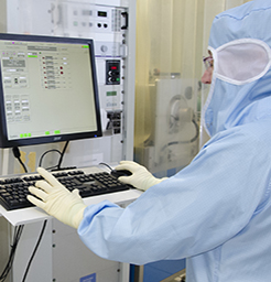
Electromagnetic and quantum design of the antennas and of the photo-detectors active region respectively, with the help of available finite element codes. Main goal: obtain a reliable model for the prediction of the electronic transport and for the optimization of the responsivity as a function of temperature and doping density.

Fabrication in clean-room environment (e-beam lithography, e-beam evaporation, plasma enhanced chemical vapor deposition, ICP etching etc)

Electrical and optical characterization of the photodetectors, through
FTIR spectroscopy
Optical mixing of MIR quantum cascade lasers [1]

Required skills Motivated PhD fellow, capable of bringing new ideas.

Good attitude towards team-work.

Solid knowledge of electromagnetics, quantum mechanics and optoelectronic devices

Experience with finite element electromagnetic simulation codes is a plus

Experience in programming for instrumentation control (Labview, Phyton) desired.

Good level of English, spoken and written.

Good writing skills (writing of papers and reports) are highly desired


Host Unit:
IEMN UMR CNRS 8520
Avenue Poincaré
59652 VILLENEUVE D'ASCQ CEDEX
www.iemn.fr

Start date:
September-December 2023.

Applications should be sent to:

Stefano Barbieri
stefano.barbieri@iemn.fr
Stefano Barbieri - web page

Stefano Barbieri
stefano.barbieri@iemn.fr
Stefano Barbieri - web page

[1] M. Hakl et al, "Ultrafast Quantum-Well Photodetectors Operating at 10 μm with a Flat Frequency Response up to 70 GHz at Room Temperature," ACS Photonics, 2021, doi: 10.1021/acsphotonics.0c01299.
[2] D. Palaferri, et al. "Room-temperature 9-μm wavelength photo- detectors and GHz-frequency heterodyne receivers," Nature 85, 556 (2018)
[3] N. A. Macleod, et al. "Broadband standoff detection of large molecules by mid-infrared active coherent laser spectrometry," Opt. Expr. 23, 912 (2015)
[4] H. Dely et al, "10 Gbit s-1 free space data transmission at 9 μm wavelength with unipolar quantum optoelectronics," Laser Photon. Rev. 16, 2100414 (2022).
[5] D. Maes et al. "High-speed UTC photodiodes on silicon nitride," APL. Photon. 8, 016104 (2022)
[6] D. D.S.Hale, et al. "The Berkeley infrared spatial interferometer: a heterodyne stellar interferometer for the mid-infrared," Astrophys. J. 537, 998 (2000)

NEWS

Assistant engineer in instrumentation and experimental techniques

Typical job
C3B41 - Assistant Engineer in Instrumentation and Experimental Techniques
Missions Reporting to the head of the "Etching" resource, the member of staff will be responsible for ensuring the smooth running of the etching machine park, developing thin-film etching processes and, as part of a quality approach, developing calibration processes for thin-film etching. He or she will be responsible for keeping a technological watch on these resources and, in collaboration with the IEMN's research teams, will be tasked with developing, guaranteeing the long-term future of and promoting innovative processes in these various etching fields.
Activities The job will involve mastering and developing expertise and know-how in the etching of thin-film materials. In particular, this involves:

  • Provide technical and scientific support for engraving equipment (DRIE, RIE, ICP)
  • Maintain this equipment.
  • Development of calibration procedures.
  • Expertise in component manufacturing tools (lithography, deposition, etching) and characterisation methods (electron microscopy, ellipsometry, profilometry, AFM, etc.).
  • Keeping a technology watch.
Qualifications: To fulfil this role, the assistant engineer will need to have sound knowledge and skills:

  • General knowledge of chemistry and physical sciences
  • Knowledge of manufacturing techniques (engraving, lithography, deposits)
  • General knowledge of instrumentation and physical measurements
  • Knowledge of vacuum techniques (primary vacuum, secondary vacuum)
  • Handling of gases under pressure
  • Aptitude for teamwork and multi-project objectives
  • General knowledge of health and safety rules
  • Mastery of the English language: oral and written expression and comprehension.
Context: The assistant engineer will work in the micro and nanomanufacturing centre at the IEMN Central Laboratory (LCI) in Villeneuve d'Ascq. He/she will report to the IEMN's Technical Director, who is responsible for the platform.

The IEMN is a 450-strong research institute. Its multidisciplinary research activities cover a broad spectrum, from materials physics to telecommunications systems.

Its research activities are based mainly on five technical services: the Micro and Nano Fabrication Centre (CMNF), the near-field microscopy platform, the HF-MEMS (Micro-Electro-Mechanical-Systems) electrical characterisation centre, the telecoms platform and the EMC (Electro-Magnetic Compatibility) platform.


Host Unit:
IEMN UMR CNRS 8520
Avenue Poincaré
59652 VILLENEUVE D'ASCQ CEDEX
www.iemn.fr

Contract Type:
Technical CDD

Duration of the contract :
3 months

Expected date of hire:
2 May 2019

Number of hours worked :
Full-time

Compensation:
gross monthly salary
according to experience

Desired level of education:
BAC + 2

Desired experience :
3/5 years

For further information
If you are interested in this position, please contact
bertrand.grimbert@univ-lille.fr

Logo
Cité Scientifique
Avenue Henri Poincaré
CS 60069
59 652 Villeneuve d'Ascq Cedex, France
Tel : 03 20 19 79 79
CNRS Logo University of Lille Logo University Polytech Logo Junia Logo Centrale Lille Logo Renatech Logo RFnet Logo
Site map
Copyright Service ECM et pôle SISR 2024
  • Scientific production
  • Legal information
  • Privacy policy
Faire défiler vers le haut
fr_FR
fr_FR
en_GB
We use cookies to ensure you have the best experience on our website. If you continue to use this site, we will assume that you are happy with it.OKNoPrivacy policy