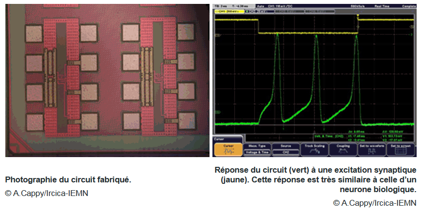
As Moore’s law reaches its end, traditional computing technology based on the Von Neumann architecture is facing fundamental limits. Among them is poor energy efficiency. This situation motivates the investigation of different processing information paradigms, such as the use of spiking neural networks (SNNs), which also introduce cognitive characteristics. As applications at very high scale are addressed, the energy dissipation needs to be minimized. This effort starts from the neuron cell. In this context, this paper presents the design of an original artificial neuron, in standard 65 nm CMOS technology with optimized energy efficiency. The neuron circuit response is designed as an approximation of the Morris-Lecar theoretical model. In order to implement the non-linear gating variables, which control the ionic channel currents, transistors operating in deep subthreshold are employed. Two different circuit variants describing the neuron model equations have been developed. The first one features spike characteristics, which correlate well with a biological neuron model. The second one is a simplification of the first, designed to exhibit higher spiking frequencies, targeting large scale bio-inspired information processing applications. The most important feature of the fabricated circuits is the energy efficiency of a few femtojoules per spike, which improves prior state-of-the-art by two to three orders of magnitude. This performance is achieved by minimizing two key parameters: the supply voltage and the related membrane capacitance. Meanwhile, the obtained standby power at a resting output does not exceed tens of picowatts. The two variants were sized to 200 and 35 μm2 with the latter reaching a spiking output frequency of 26 kHz. This performance level could address various contexts, such as highly integrated neuro-processors for robotics, neuroscience or medical applications.
Introduction
Computing technology, based on binary coding, Von Neumann architecture and CMOS technology, is currently reaching certain limits (Waldrop, 2016). Traditional computers, the champions for the resolution of complex equation systems, have difficulties to classify/organize data, something that the human brain seems to accomplish effectively. For this reason, research in the field of Artificial Neural Networks (ANNs) is attracting much attention and is quickly developing worldwide. At the bottom of these efforts lies the ultimate goal to realize machines that could surpass the human brain, in some aspects of cognitive intelligence. In that sense, brain research and ANNs bear the promise of a new computing paradigm.
Currently, traditional, discrete-time, digital ANNs, fueled by the unprecedented computational capability of modern Graphics Processing Units (GPUs), represent the state-of-the-art for addressing cognitive tasks (Oh and Jung, 2004; LeCun et al., 2015) such the ones encountered in computer vision applications. However, it is the more recent class of Spiking Neural Networks (SNNs), often referred to as the third generation of neural networks, that are known to be bio-realistic and more computationally potent compared with their predecessors (Maass, 1997). The functional similarity with the actual biological networks permits envisioning, apart from interfacing or reproducing brain processes, the implementation of circuits and systems with cognitive characteristics without explicit programming tasks. This would endow the modern generation of computers with the capacity to learn from input data.
In SNNs, neuronal communication is carried out in the form of noise-robust, signal pulses or “spikes.” SNNs try to reproduce the physical characteristics of the brain, through highly connected neurons dendrites and axons. At present, two main methodologies fulfill neuro-inspired computing tasks: digital simulation and hardware implementation.
In digital simulations, the dynamics of neuronal models are coded in software and calculated on general-purpose digital hardware. Digital simulations have the advantage that they can be reliably programmed using numerical operations of very high precision. However, their reliability comes at the cost of high circuit complexity, which is necessary for the data transfer, exchange and processing (Cao et al., 2015). Accordingly, the energy consumption remains still very high, especially as one juxtaposes biological data for comparison. For instance, the brain of the cat is emulated at the cost of a power dissipation in the megawatt range (Ananthanarayanan et al., 2009), while the animal brain actually consumes only a couple of watts.
As far as hardware implementations of SNNs are concerned, the alternative, “neuromorphic,” approach consists of employing VLSI circuit technology, namely CMOS fabrication processes which can be possibly associated with more advanced device technology such as memristors (Kim et al., 2012). The analog hardware approach consists of a large-scale integration of silicon artificial neurons (AN) and synapses, in an attempt to produce low power neuro-inspired architectures compatible with the current electronics technology.
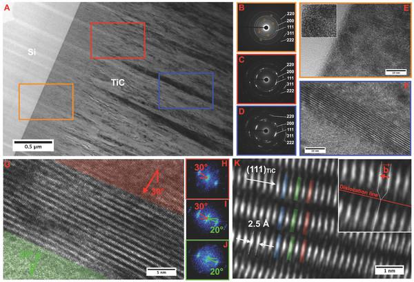
The efficiency of such architectures can be revealed in contrast to the energy consumption of biological neurons (BN). Brain activity needs a continuous exchange of ions through the cell membrane and these exchanges correspond to the charge and discharge of the neuron capacitance (soma, dendrite, and axon). As a consequence, the important parameters for energy dissipation are the membrane capacitance and the voltage swing. Membrane capacitance varies considerably according to the type of neuron cell, ranging from picofarads to nanofarads for the largest ones (Amzica and Neckelmann, 1999; Golowasch et al., 2009; Rössert et al., 2009; Tripathy and Gerkin, 2012). Interestingly, a recent estimation of the capacitance that could be involved for computation in the human cortex is proposed in Hasler and Marr (2013). The calculations are based on a digital power model and suggest a biological system of 1012 neurons with a 0.5 Hz average firing rate. The total capacitance value is calculated at 245 pF that is high when compared with the femtofarad order common in integrated circuits. Indeed, energy savings could be envisioned in silicon AN by aiming at reducing the capacitance and/or the voltage swing.
Next to a reduced capacitance, low power operation in silicon neurons can be facilitated by the physics of the MOS transistors. Indeed, as it has been observed (Mead, 1989, 1990) the nervous system uses, as its basic operation, a current that increases exponentially with the membrane voltage, similar to the current-voltage characteristic of a MOS transistor operating in subthreshold. However, the physical origins of these exponential dependencies are very different: a non-linear voltage controlled conductance in biological membrane against a current controlled by an energy barrier in the transistor. Due to this, the MOS transistor can only asymptotically approach a slope of kT/q per e-fold of current change, while the biology is not limited as such (Mead, 1989, 1990). Even if I-V characteristics show different slopes, a bridge between the physics of biological membrane and the one of electronic devices has been established, especially when the energy and power properties are considered. This led to the advent of neuromorphic silicon neurons, which allowed neuronal spiking dynamics to be directly emulated on analog large-scale integration chips. So far, several generations of SNNs have been proposed and the reader could refer to the relevant works (Misra and Saha, 2010; Indiveri et al., 2011; Hasler and Marr, 2013) to obtain more information.
Based upon these previous works, this paper describes the design and measurement results of a new family of silicon AN. It was designed under the guidelines of (i) a biophysically meaningful model, (ii) a minimum energy dissipation, (iii) an analog circuit that would allow a complete time variation modeling of the membrane potential and (iv) a resulting topology, that when implemented in CMOS technology, it would occupy a minimum area in order to enable large scale integration. This unique combination of characteristics resulted in a neuron topology that was measured to consume several orders of magnitude less energy than the values encountered either for BN or the AN reported so far.
The rest of this paper is organized as follows: The “Materials and methods” section will be devoted to a discussion on neuron energy efficiency, the selection of the mathematical model and the circuit topology and functionality. The circuit proposed in this paper was fabricated and characterized experimentally. Both simulation and experimental results are described in the “Results” section. The “Discussion” section presents a comparison with the state of the art and highlights issues regarding noise, supply voltage sensitivity and temperature impact. Finally conclusions are drawn in the eponymous last section.

 The state-of-the-art of terahertz (THz) sources based on quantum cascade heterostructures will be reviewed from the viewpoint of short pulse generation. There are two principal applications of the concept of quantum cascade – for the emission and for the detection of terahertz waves. On the emitter’s side, THz quantum cascade lasers (QCLs) are increasingly exploited for sensing and imaging applications. Today QCLs span a frequency range from 1.8THz to 5 THz with record peak output powers of 1 W and CW single-mode average powers in the 100s mW range. Recently, a concept of heterogeneous QCL active region has been successfully implemented leading to broadband emission over one octave and even to frequency comb operation with a 600 GHz bandwidth. Such active medium can be used for the generation of short (bandwidth limited) pulses.