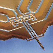
Vmicro, spinoff de l’IEMN réalise la configuration verticale du premier microscope de champ proche de l’histoire

APPLIED PHYSICS LETTERS 110, 243101 (2017) [http://dx.doi.org/10.1063/1.4985125]
Instrumentation aux limites : le nouveau microscope à force atomique renouvelé par les capteurs micro-et nano- systèmes, basé sur un microsystèmes
Tes microscopes sont des outils de travail quotidiens dans des domaines tels que l’électronique, la chimie, la métallurgie, les sciences de la vie, la recherche en physique. Disposer de microscopes performants est indispensable pour créer de nouvelles filières technologiques (qualifier les matériaux, les procédés) ou encore poser un diagnostic. Bien que très répandus, les microscopes optiques ne suffisent pas toujours à fournir la résolution nécessaire a cause des limites imposées par la diffraction de la lumière.
Une troisième famille de microscopes, dits à sondes locales, a vu le jour dans les années 1980. La technologie la plus répandue est le microscope à force atomique ou AFM pour Atomic Force Microscope. Son principe revient à remplacer le sens de la vue par celui du toucher. Une nano-pointe balaye la surface à observer ligne par ligne, à la manière des non-voyants lisant le braille. La pointe renvoie une mesure de force, et, en assemblant toutes les lignes, le microscope reconstitue une image de la surface. Grâce aux micro-technologies, on sait fabriquer depuis 1985 des pointes extrêmement fines. Cela confère au microscope AFM une résolution lui permettant de voir des nanostructures, des atomes individuels, ou encore des molécules (ADN, protéines). Cependant, jusqu’à maintenant le capteur de force qui fait le lien entre la pointe et la tête de l’appareil avait très peu évolué: il limitait fortement la rapidité de la mesure et nécessitait une instrumentation optique macroscopique qui constitue souvent un verrou.
Depuis 2005, les travaux de l’IEMN sur des technologies MEMS (Micro-Electro-Mechanical-Systems ont permis d’explorer une instrumentation basée sur des capteurs renouvelés. Cette approche est repartie à la base par la conception micromécanique de résonateurs à pointes, puis s’est poursuivie sur les aspects instrumentaux.
En 2015, la société Vmicro a été créée en tant que spin-off du laboratoire et poursuit le développement de ces sondes en optimisant toutes les étapes de fabrication en salle blanche, afin de mettre sur pied une production compatible avec les exigences des utilisateurs d’AFM issus de domaines très variés, de la science des surfaces aux biologistes. L’entreprise collabore à travers plusieurs projets avec l’IEMN et une publication commune vient de concrétiser un nouveau saut technologique.
Tes chercheurs et ingénieurs ont développé une micro-sonde verticale basée sur un résonateur qui permet de contrôler le mouvement de la pointe de façon optimale et ce à des fréquences de plusieurs mégahertz. Une version plus miniature en technologie NEMS est aussi présentée dans l’article.
Te nouveau capteur, nommé Vprobe, a été utilisé dans un microscope commercial modifié et a été testé avec succès en conditions réelles, aux limites instrumentales permises par le montage. Avec une pointe très élancée, la Vprobe réalise enfin la configuration verticale du premier microscope de champ proche de l’histoire, le STM (scanning tunneling microscope) mais avec les atouts de l’AFM. Des transducteurs inventés pour l’occasion permettent de travailler à très faible impédance.
Référence : Atomic force microscope based on vertical silicon probe – APPLIED PHYSICS LETTERS 110, 243101 (2017)
Benjamin Walter,1 Estelle Mairiaux,1 and Marc Faucher1,2
1 – Vmicro SAS, Avenue Poincaré, 59650 Villeneuve d’Ascq, France
2 – Institut d’Electronique, de Microélectronique et de Nanotechnologie, CNRS UMR 8520, Univ. Lille
ABSTRACT : A family of silicon micro-sensors for Atomic Force Microscope (AFM) is presented that allows to operate with integrated transducers from medium to high frequencies together with moderate stiff- ness constants. The sensors are based on Micro-Electro-Mechanical-Systems technology. The verti- cal design specifically enables a long tip to oscillate perpendicularly to the surface to be imaged. The tip is part of a resonator including quasi-flexural composite beams, and symmetrical transducers that can be used as piezoresistive detector and/or electro-thermal actuator. Two vertical probes (Vprobes) were operated up to 4.3 MHz with stiffness constants 150 N/m to 500 N/m and the capa- bility to oscillate from 10 pm to 90 nm. AFM images of several samples both in amplitude modula- tion (tapping-mode) and in frequency modulation were obtained. Published by AIP Publishing. [http://dx.doi.org/10.1063/1.4985125]
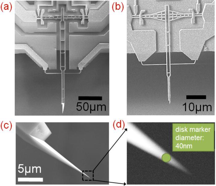
SEM images of two micro-fabricated Vprobes.
(a) Vprobe n »1 made on 5 lm device layer SOI wafer: operating frequency 1.18 MHz, stiffness 500 N/m. On this probe, the tip has an electrical access, thanks to metal lines deposited onto lateral beams 4,5.
(b) More miniaturized device Vprobe n »2 made on 500nm thick SOI: operating frequency 4.3 MHz, 150 N/m.
(c) Integrated high aspect ratio silicon tip obtained on Vprobe 1
(d) zoom at the tip apex.
 « Nos projets prennent une nouvelle dimension en s’appuyant sur l’appareil industriel éprouvé du groupe Digigram : industrialisation, commerce, marketing, logistique – nous poursuivons et accélérons notre développement Notre identité portée par l’innovation, au plus près du terrain, a rencontré un partenaire qui parle le même langage : le Groupe Digigram porte les valeurs d’audace, de passion et d’ouverture qui nous permettent de déployer nos ailes un peu plus dans le domaine de la surveillance acoustique et donne une nouvelle dynamique à l’orientation “critical audio” portée par Digigram.