Atelier consacré à la préparation des substrats pour l’épitaxie


du 22 au 24 mai 2018
IEMN – Villeneuve d’Ascq

Abstract:

La préparation des substrats (nettoyage, rugosité de surface, désoxydation, structuration, etc…) est une étape importante pour la qualité des couches semiconductrices épitaxiées. Elle est devenue cruciale alors que les recherches actuelles s’orientent vers des sujets tels que l’hétéroépitaxie sur Silicium, l’épitaxie latérale ou celle de nanostructures (par croissance sélective avec masque diélectrique, par gravure de la surface du substrat ou par dépôt de nanoparticules métalliques permettant la croissance catalysée de nanofils). Durant cet atelier du GDR PULSE, ces différentes thématiques seront abordées afin d’échanger à partir des présentations invitées sur nos différentes méthodes de préparation et sur les moyens les plus adéquats pour les caractériser.

affiche_atelier_epitaxie

https://atelier-pulse.sciencesconf.org

Thesis: Study of non-stoichiometric III-V semiconductors for sampling microwave signals

Thomas Demonchaux
Thesis defence

16 May 2018 at 10:30 a.m.
IEMN Amphitheatre - Villeneuve d'Ascq

Abstract:

Discovered in the late 1980s, low-temperature epitaxial gallium arsenide (GaAs-BT) has interesting properties for optoelectronic applications. Its properties are closely linked to the presence of point defects, the deep levels of which give lifetimes compatible with its use as an active layer in photo-switches. With the aim of improving current knowledge of the physical origin of the lifetime and thus optimising it, this thesis work involved carrying out an in-depth study of the material, in particular by combining macroscopic analyses with microscopic characterisation. It is divided into five chapters, the first of which presents the current state of knowledge of GaAs-BT, while the second describes the various techniques used in this study. The third chapter looks at the chemical composition of the low-temperature epitaxial layer and its structural characterisation by X-ray diffractometry. It reveals the growth of ternary or quaternary compounds highly diluted in phosphorus and indium and suggests the presence of V-element antisites. The presence of phosphorus raises the question of the chemical nature of these antisites. The next chapter aims to identify the point defects embedded in the material using low-temperature scanning tunneling microscopy. Although the majority of the defects differ from the antisites observed in the literature by having a negative charge state and a changing appearance when the tip passes through, an analysis of the imaging conditions as a function of temperature combined with ab-initio calculations indicates the preferential formation of arsenic antisites compared with phosphorus antisites. The final chapter is devoted to the characterisation of the material after annealing. The particularity of this section lies in the discovery that the antisites do not precipitate at a growth temperature of 325°C and therefore give the most interesting lifetimes for the desired applications.

Jury members :

Mr Alain Le Corre
Mr Georges Bremond
Mr Didier Stiévenard
Mr Stéphane Formont
Mr Bruno Grandidier
Mr Xavier Wallart
Professor, INSA Rennes
Professor, INSA Lyon
Director of Research, CNRS, IEMN
Engineer, Thalès
Director of Research, CNRS, IEMN
Rapporteur
Rapporteur
Member
Member
Director
Co-director


Seminar: RF-Sensors in Advanced Applications

Dr.-Ing. Christoph BAER & Ing. Birk HATTENHORST
Institute of Electronic Circuits
Ruhr-Universität Bochum, Universitätsstr. 150, ID 03/324
44780 Bochum - GERMANY

Monday 23 April 2018 at 2.00 pm
IEMN Boardroom - Villeneuve d'Ascq

Abstract:

RF-sensors and Radar systems found their way into civil and industrial applications decades ago. Since then, they reliably measure distances, velocities, and filling levels etc. contact free and with great accuracy. Lately, current trends and technological achievements pushed operating frequencies up to the millimeter wave range, which allows for the determination of various additional physical quantities. Consequently, these novel sensors can be utilized in numerous areas of process industry, civil protection, and daily life. Therefore, their main purpose will be the determination and investigation of environmental parameters that allow for the supervision of crucial system parameters and the interpretation of complex processes. The talk will give an overview on diverse RF-sensors for different applications, which were explored at the Ruhr-University Bochum within recent years. The presented sensor applications include: humanitarian demining, mmWave imaging, contact-free gas sensing, as well as dust and particle determination for process industry and natural hazard protection. Next to the introduction of the numerous areas of application, the different sensor designs will be explained and their field applicability verified. Moreover, opportunities regarding student exchanges between Ruhr-University and Lille University will be introduced and discussed.

About the lecturers:
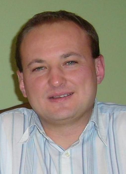
Christoph Baer received his diploma and doctor degree in electrical engineering at Ruhr-University Bochum in 2009 and 2015, respectively. From 2006 to 2015 he worked as a research engineer on radar systems and radar applications with the Krohne Group in Duisburg, Germany. Currently, Dr. Baer is postdoctoral researcher and academic counselor with the Institute of Electronic Circuits at Ruhr-University Bochum. He is author or co-author of more than 60 international publications and holds 8 international patents. His research interests include ground penetrating radar systems and concepts, methods for humanitarian demining, RF-material characterization and synthesis, sensors for avalanche science, and industrial microwave sensors. Dr. Baer is chairman of the IEEE SIGHT Germany Section.


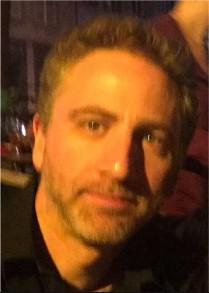
Birk Hattenhorst was born in Lübbecke, Germany, in 1989. He received the M.Sc. degree in electrical engineering from the Ruhr-University Bochum, Bochum, Germany, in 2014. He has been a Research Assistant with the Institute of Electronic Circuits, Ruhr-University Bochum, since 2014. His current research interests include microwave measurement techniques, radar technology, antenna design, meta-materials and material characterization.

Séminaire : Innovative Colloidal Nanostructures: Nanoplatelets and III-V Quantum Dots

tessier_mickaelDr Mickaël Tessier
Ghent university, Belgium

Mercredi 17 avril 2018 à 14h00
IEMN Boardroom - Villeneuve d'Ascq

Abstract:

Innovative Colloidal Nanostructures: Nanoplatelets and III-V Quantum Dots
Colloidal Quantum Dots (QDs) are semiconductor nanocrystals in the 1 to 10 nm size range synthesized by wet chemistry process. Because of these small sizes, QDs are subject to quantum-size effect. This effect leads to discrete transitions, much like in an atom or a molecule, with energies higher than the bulk and that are strongly dependent of the QDs sizes. This property has allowed QDs to emerge as a novel class of optoelectronic materials over the last 25 years. The most advanced application of colloidal QDs, at least from a research valorization perspective, is their commercial use in liquid crystal displays (LCDs). First launched in 2013, sales of QDs-enhanced LCDs are expected to achieve 18 million units in 2018.
a. Vials containing QDs of different sizes under UV light. The emitted color depends of the QDs sizes. b. Commercial QDs display (http://www.samsung.com/global/tv/).
Significant advances have been made in the synthesis of QDs since the beginning of the 1990s. The shape of the nanoparticles can now be finely controlled, and nanoparticles with various shapes have been synthesized. In particular, colloidal nanoplatelets are atomically flat nanostructures that present only one dimension of quantum confinement.1In this lecture, I first present how the nanoplateletssizeand composition can be perfectly controlled via inventive synthesis protocols and how theseparameters affects the nanoplatelets optical properties.(2–4)
To facilitate the use of nanocrystals in the industry, interest is shifting from the well-characterized cadmium-based QDs to cadmium-free alternatives such as indium phosphide. We recently proposed protocols based onaminophosphine-type precursors that allow for a cost efficient, up-scaled syntheses of indium phosphide(InP) QDs of different sizes.(5) A detailed understanding of the reaction chemistry is a key in the development of colloidal QDs synthesis. I present an investigation of chemical reactions leading to the formation of InP starting from aminophosphine-type precursors.(6) This mechanism is innovative in the sense that it points out a double role of the phosphorus precursor in the reaction as both a reducing agent and the source of the phosphorus needed to form InP. Its understanding furthers the general use of aminopnictogens for the
synthesis of III-V QDs.(7) Finally, I show that InP QDs can be processed in polymer layer and that their structure can be optimized in order to obtain more efficient and cheaper lighting devices.(8)

References
(1) Ithurria, S.; Tessier, M. D.; Mahler, B.; Lobo, R. P. S. M.; Dubertret, B.; Efros, A. L. Nat. Mater.2011, 10, 936–941.
(2) Tessier, M. D.; Mahler, B.; Nadal, B.; Heuclin, H.; Pedetti, S.; Dubertret, B. Nano Lett.2013, 13, 3321–3328.
(3) Tessier, M. D.; Spinicelli, P.; Dupont, D.; Patriarche, G.; Ithurria, S.; Dubertret, B. Nano Lett.2014, 14, 207–213.
(4) Tessier, M. D.; Javaux, C.; Maksimovic, I.; Loriette, V.; Dubertret, B. ACS Nano2012, 6, 6751–6758.
(5) Tessier, M. D.; Dupont, D.; De Nolf, K.; De Roo, J.; Hens, Z. Chem. Mater.2015, 27, 4893–4898.
(6) Tessier, M. D.; De Nolf, K.; Dupont, D.; Sinnaeve, D.; De Roo, J.; Hens, Z. J. Am. Chem. Soc.2016, 138, 5923–5929.
(7) Grigel, V.; Dupont, D.; De Nolf, K.; Hens, Z.; Tessier, M. D. J. Am. Chem. Soc.2016, 138, 13485–13488.
(8) Dupont, D.; Tessier, M. D.; Smet, P. F.; Hens, Z. Adv. Mater.2017, 29, 1700686.

Les mardis de l’Innovation : L’enjeu global du stockage de l’énergie

pour l’avenir de l’internet des objets, des énergies alternatives et de la mobilité.
Christophe LETHIEN, Institut d’Electronique, de Microélectronique et de Nanotechnologie, Université de Lille, CNRS.
Les Mardis de l’innovation. 20 Mars 2018.

> Visionnez la conférence sur vimeo

 Véritable encyclopédie vivante de l’innovation à travers le monde, destinée aux acteurs de l’innovation. Les Mardis de l’Innovation sont des cours/conférences en format ouvert portant sur la culture de l’innovation et sa mise en œuvre entrepreneuriale. Depuis dix ans, 270 cours/conférences, plus de 600 professionnels formés, plus de 10 000 auditeurs libres, 200 témoignages d’entreprises parmi les plus innovantes au monde.


IEMN : CS Industry Award

Rewarding excellence, innovation and success

La compagnie ALLOS semiconductors s’est vu décerner un CS Award portant sur des travaux effectués en étroite collaboration avec l’équipe de recherche du Dr Farid Medjdoub de l‘Institut d’électronique, de microélectronique et de nanotechnologie. Les derniers résultats de l’IEMN démontrent notamment une tension de claquage de plus de 1400 V pour les mesures verticales et latérales sur le prochain produit d’ALLOS, l’épiwafer GaN-on-Si pour les appareils de 1200 V.

H.D.R. Contributions à la compréhension du canal de propagation sans-fil MIMO : modèles, applications et perspectives – GAILLOT, DAVY

DAVY GAILLOT
HDR HABILITATION A DIRIGER DES RECHERCHES

Le 27 mars 2018 à 10h30
Ecole doctorale : Sciences Pour l’Ingénieur (SPI)
Laboratoire/Etablissement : IEMN-IRCICA, Université de Lille – FST

Amphithéâtre 1A12 – IUT-A

Discipline : SCIENCES PHYSIQUES

Abstract:

Ce mémoire d’HDR retrace 9 années d’études théoriques et expérimentales sur la compréhension physique des mécanismes de propagation dans les canaux radiofréquences MIMO complexes indoor et outdoor, les modèles, ainsi que les applications.
Les mécanismes de propagation et le canal radio polarimétrique MIMO sont d’abord présentés ainsi que la problématique liée à la faiblesse du modèle purement spéculaire. Dans un deuxième temps, les techniques de sondage de canal et équipements
utilisés pour mesurer le canal radio sont discutés et la complémentarité avec le modèle spéculaire est mise en lumière. De plus, l’estimateur paramétrique polarimétrique MIMO reposant sur la technique de maximum de vraisemblance déterministe pour la composante spéculaire et stochastique pour la composante dense est détaillé. Une analyse complète des mécanismes polarimétriques est ensuite présentée en milieu industriel à 1.3 GHz et en milieu confiné autour de 60 GHz. Ces analyses ont été le préambule au développement de modèles polarimétriques incluant la composante dense traitant de l’atténuation (path loss) et du profil en puissance des retards (PDP). Ces aspects de modélisation et l’ensemble des outils développés se sont inscrites
principalement dans le cadre d’applications telles que la localisation de mobiles en milieu outdoor ou encore l’exposition aux ondes électromagnétiques en milieu confiné. Enfin, nous terminerons ce mémoire en présentant les nombreuses perspectives de recherche qui s’articulent principalement autour de la caractérisation dynamique du canal radio MIMO et MIMO massif (massive MIMO) pour des applications V2V avec des fréquences jusque 6 GHz dans le cadre du pôle de compétitivité transports de la Région des Hauts-de-France, du canal THz MIMO pour des applications de télécommunications à très haut débit dans le cadre de la 5G, mais également des nouveaux travaux originaux sur l’interaction des ondes électromagnétiques avec des cellules vivantes.

Jury members :

Garant de l’habilitation :

  • MME. LIENARD Martine, Professeure de l’Université de Lille – FST

Rapporteurs :

  • M. BENLARBI-DELAI Aziz, Professeur de Sorbonne Université
  • M. EL ZEIN Ghaïs, Professeur de l’INSA Rennes
  • M. VAUZELLE Rodolphe, Professeur de l’Université de Poitiers

Examiners :

  • M. CLAVIER Laurent, Professeur de l’Institut Mines TELECOM Lille-Douai
  • M. OESTGES Claude, Professeur de l’Université Catholique de Louvain, Belgique
  • SOUTENANCE : Mardi 27 Mars 2018 à 10h30, IUT-A Amphi 1A12

HDR_2018_Davy Gaillot

Seminar: Molecular spin coupling at the tip of an STM

By Laurent Limot
CNRS researcher at the IPCMS in Strasbourg
Contact: limot@ipcms.unistra.fr

Wednesday 16 April 2018 at 10.30 a.m.
IEMN Boardroom - Villeneuve d'Ascq


Abstract:

Recent advances in addressing and controlling the spin states of a surface-supported object (atom or molecule) have further accredited the prospect of quantum computing and of an ultimate data-storage capacity [1]. Information encoding requires that the object must possess stable magnetic states, in particular magnetic anisotropy to yield distinct spin-dependent states in the absence of a magnetic field together with long magnetic relaxation times. Scanning probe techniques have shown that inelastic electron tunneling spectroscopy (IETS) within the junction of a scanning tunneling microscope (STM) is a good starting point to study the stability of these spin states [2]. STM-IETS allows for an all-electrical characterization of these states by promoting and detecting spin-flip excitations within the object of interest. As spin excitations need however to be preserved from scattering events with itinerant electrons, single objects are usually placed on non-metallic surfaces such as thin-insulating layers or superconductors. In this sense, new approaches to improve the detection of spin-flip excitations are desirable. With this purpose we present here a novel strategy based on the molecular functionalization of a STM tip. We study the surface magnetism of a simple doubledecker molecule, nickelocene [Ni(C5H5)2], which is adsorbed directly on a copper surface. By means of X-ray magnetic circular dichroism and density functional theory calculations, we show that nickelocene on the surface is magnetic (Spin = 1) and possesses a uniaxial magnetic anisotropy, while IETS reveals an exceptionally efficient spin-flip excitation occurring in the molecule [3]. Interestingly, nickelocene preserves its magnetic moment and magnetic anisotropy not only on the surface, but also in different metallic environments. Taking advantage of this robustness, we are able to functionalize the STM tip with a nickelocene [3,4], which can then be employed as a portable source of inelastic excitations. As we will show during the talk, IETS can then be used to probe the interaction between a surface-supported object and the nickelocene tip, including a magnetic interaction.

M. Ormaza1, P. Abufager2, B. Verlhac1, N. Bachellier1, M.-L. Bocquet3, N. Lorente4, and Laurent Limot1,*
1Université de Strasbourg, CNRS, IPCMS, UMR 7504, F-67000 Strasbourg, France
2Instituto de Física de Rosario, CONICET, Universidad Nacional de Rosario, Argentina
3Ecole Normale Supérieure, UPMC Univ. Paris 06, CNRS, 75005 Paris, France
4CFM/MPC and DIPC, 20018 Donostia-San Sebastián, Spain

References
[1] F.D. Natterer et al, Nature 543, 226 (2017); T. Choi et al, Nat. Nanotech. 6 (2017)
[2] A.J. Heinrich, J.A. Gupta, C.P. Lutz, and D.M. Eigler, Science 306, 466 (2004)
[3] M. Ormaza et al, Nano Lett. 17, 1877 (2017)
[4] M. Ormaza et al, Nat. Commun. 8, 1974 (2017)


Conference: Prototype of Terahertz Communications at 300 GHz: Devices, Packages

HO-JIN-SONG_Pohang_University_of_Science_and_Technology-POSTECHDr. HO-JIN SONG, Pohang University of Science and Technology (POSTECH)Korea

Tuesday 6 April at 14h00

Anfiteather - IEMN-LCI Institut d'Electronique, de Microélectronique et de Nanotechnologie U.M.R C.N.R.S 8520 - Laboratoire Central - Cité Scientifique - Avenue Poincaré - CS 60069 - 59652 VILLENEUVE D'ASCQ CEDEX

Abstract:

Thanks to the significant advances made in wireless communications technologies over the last couple of decades, radio communications systems are now being used to deliver not only simple text or voice messages but also multimedia information and real-time streaming of video through the internet anytime and anywhere. However, the steady progress cannot fulfill the recent needs from both industry and end-users. Many leaders of industry are expecting new applications, such as virtual reality, a tactile internet, connected cars, remote surgery, and the internet of everything, that would cause a paradigm shift in key industries. The requirements for such applications include higher throughputs to deliver or collect huge amounts of information from all intelligent things, low latency to maintain mission critical even through wireless networks, and the capability of massive connectivity. The most straightforward way to satisfy these requirements is to provide more spectral bandwidth, which is the most fundamental resource in wireless communications. In recent discussions of the 5G system, there has been a strong consensus among the parties to deploy millimeter-wave radio access technology, which is expected to offer an order of magnitude larger bandwidth at minimum. For further future applications, such as terabit connectivity or terabit wireless, even higher frequencies, in particular those above 275 GHz, which have never been discussed for any commercial use yet, are attracting increasing interest because of the huge spectral area. The available bandwidth in the THz region is definitely much wider than the entire spectral resources utilized for all wireless systems on this planet.
Recent progress in semiconductor devices on compound semiconductor or silicon substrates has made it possible to produce more power and receive a signal with less noise at THz frequencies. Various integrated circuits for the THz radio front-end functional blocks, including power and low-noise amplifiers, modulators and demodulators, and oscillators, have been demonstrated in the last decade. In the first experimental demonstration conducted in 2004, bulky instruments originally developed for THz spectroscopy were used to transmit pulsed THz signals carrying a 7-kHz bandwidth audio signal across a short free space. However, recently, there have been several successful demonstrations of multi-Gbps data transmissions at THz frequencies with state-of-the art devices and components.

In this talk, the first prototype of a THz wireless communications system designed under the 'touch-and-go' scenario will be presented. I clarify the concept of the KIOSK data downloading system, cover some considerations in this work, and present a brief link-budget plan. We will then overview technologies for implementing THz components operating at 300 GHz and their performance, followed by preliminary investigation of the channel responses and the experimental demonstration results.

Pohang-University-of-Science-and-Technology_logo

Innovation Tuesdays: The global challenge of energy storage for the future of the Internet of Things, alternative energies and mobility

Tuesday 20th March 2018

Welcome 18:00 - Conference 18:30 - 20:30
CNRS, 3 rue Michel-Ange, 75016 Paris

Energy storage technologies are at the heart of a major global challenge. The future of many innovations is linked to major advances in compact storage capacity and rapid battery recharging (cars and all other forms of mobility, including smartphones). As the major alternative energies (wind and solar) are not continuous, their effectiveness in future networks is also linked to improvements in electricity storage. As for the gigantic world of connected objects in the offing, this will require miniaturised batteries with very long lifetimes without recharging. While lithium is currently the leading material, with a wide range of combinations, other materials and alternative technologies such as fuel cells are making rapid progress. A journey to the heart of global competition, from advanced research into battery efficiency and recycling to access to materials, leading to a global industrial battle currently dominated by Asia.

Speakers

  • François BARSACQCEO, EasyLi, designer and manufacturer of energy storage solutions
  • Patrice SIMONElectrochemical Energy Storage Network, RS2E
  • Christophe LETHIENInstitute of Electronics, Microelectronics and Nanotechnology , IEMNUniversity of Lille, CNRS
  • Nicolas LECLERE, Head of the Electric Powertrain Innovation Division, PSA Group