IEMN
  • Home
  • News
    • IEMN Newsletters
    • M2-Ingé Internships
    • Job offers
    • All news
  • The Institute
    • Presentation
    • Organization of the institute
    • The Scientific Department
    • The Technological Department
    • Administrative and financial management
    • Rules of procedure
    • Our commitments
  • The Research
    • Scientific departments
      • Nanostructured Materials and Components
      • Micro / nano optoelectronics
      • Telecommunications Technologies and Intelligent Systems
      • Acoustic
    • Research groups
    • Flagship
  • Scientific Production
    • IEMN publications
    • Scientific production resources
  • The platforms
    • CMNF - Central Platform for Micro Nano Manufacturing
      • Engraving and implantation pole
      • In Line Analysis Unit
      • Soft Lithography and Bio Microfluidics
      • Deposits and epitaxy division
      • Lithography Unit
      • Packaging Division
      • CMNF Staff
    • PCMP - Multi-Physics Characterization Platform
      • Scanning Probe Microscopy Facility
      • Hyperfrequency, Optical and Photonic Characterization (CHOP)
      • Advanced Communications Systems and Prototyping cluster (SigmaCOM)
      • Characterisation, ElectroMagnetic Compatibility and Prototyping Centre (C2EM)
      • PCMP Staff
    • Services offered by our platforms
  • Partnership - Valuation
    • Academic Collaborations
    • ANR Projects
    • Main international collaborations
    • Industrial partnerships
    • The joint IEMN-Industry laboratories
    • Startups
  • Research Training
    • After the thesis
      • Do a post-doc at the IEMN
      • Towards the world of business and industry
      • Become a teacher-researcher
      • Become a Researcher
      • Starting a business at IEMN
      • FOCUS on a SATT engineer from the IEMN
    • A thesis at IEMN
      • Thesis and HDR defenses
      • Thesis topics
      • Financing
      • Doctoral studies
    • Master - Engineer
      • Masters ULille
        • Master Life Sciences and Technologies graduate programme
        • Master Nanosciences and Nanotechnologies - Speciality ETECH
        • Master Networks and Telecommunications
      • UPHF-INSA Masters
        • Master in Embedded Systems and Mobile Communications Engineering
        • Master Cyber Defense and Information Security
        • Master in Materials, Control and Safety
        • Master in Image and Sound Systems Engineering
      • Partner/Tutoring Engineering Schools
      • M2-Ingé Internships
    • The Lille branch of the GIP-CNFM
    • Nano-École Lille
  • Contact Us
    • Location
    • Contact form
    • Staff directory
  • Our support
  • fr_FR
  • Rechercher
  • Menu Menu
MICROSCOPIE EN CHAMP PROCHE

Pôle Microscopie en Champ Proche (PCP)

Le site internet: Air Domain

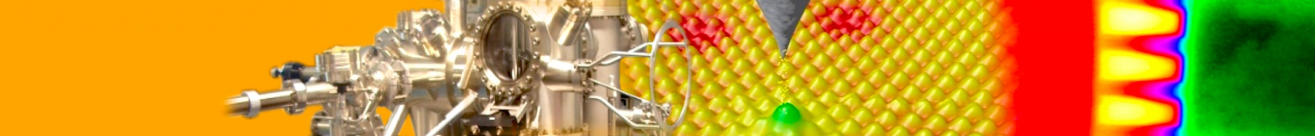
The pôle de microscopie en champ proche réunit les moyens dédiés à l’analyse topographique, physique et électrique de surfaces de 100µm jusqu’à l’échelle atomique.

L’installation PCP est organisée en deux domaines en fonction de l’environnement de mesure :

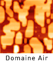
  • Le domaine AIR pour les microscopes fonctionnant dans une atmosphère ambiante d’air, de liquide ou de gaz contrôlé.
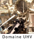
  • Le domaine UHV pour les microscopes fonctionnant sous ultravide.


Avec 8 instruments et 400m² de surface dans un environnement certifié ISO8 situé au rez-de-chaussée de l’IEMN, le centre accueille environ 30 utilisateurs experts. Une partie des instruments est en libre accès et peut être réservée en ligne. Une journée de formation pour les débutants est prévue sur demande. L’équipe est composée de 3 ingénieurs permanents fournissant des services internes, externes, académiques et industriels dans le cadre du réseau national RENATECH. Leur mission concerne également le développement de nouveaux instruments et de techniques expérimentales en collaboration avec les utilisateurs, les start-ups et les sociétés SPM.

pcp-contact@iemn.fr

Key words : 
  • Microscopie 3D,
  • SPM, STM, AFM,
  • Résolution sub-nanométrique,
  • Nanocaractérisation physique,
  • Renatech
Domaines applicatifs :
  • Nanosciences,
  • Physique des surfaces, des matériaux et des nanostructures,
  • Chimie des surfaces
Equipements de la PCP au format pdf (5,1Mo)
PCP publications
Logo
Cité Scientifique
Avenue Henri Poincaré
CS 60069
59 652 Villeneuve d'Ascq Cedex, France
CNRS Logo University of Lille Logo University Polytech Logo Junia Logo Centrale Lille Logo Renatech Logo RFnet Logo
Site map
Copyright Service ECM et pôle SISR 2024
  • Scientific production
  • Legal information
  • Privacy policy
Faire défiler vers le haut
fr_FR
fr_FR
en_GB
We use cookies to ensure you have the best experience on our website. If you continue to use this site, we will assume that you are happy with it.OKNoPrivacy policy