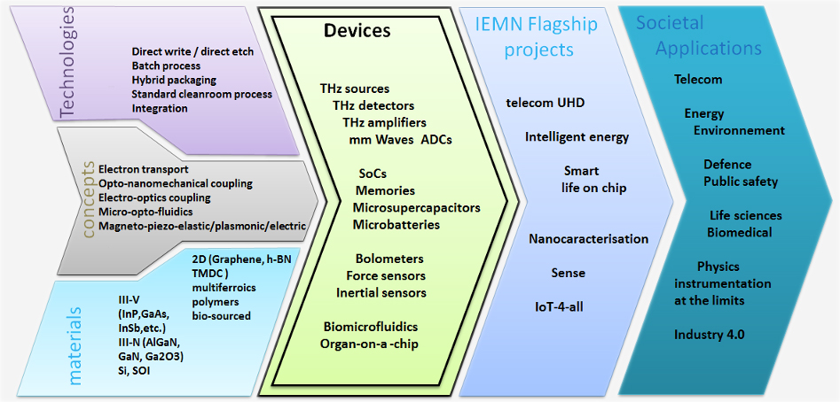
MICRO/NANO DEVICES
The IEMN is structured by flagship projects targeting societal challenges such as health, energy or telecommunications. The success of most of them will require the development of devices beyond the state of the art. These devices are fabricated using available micro and nanotechnology techniques and roadmaps, but also by developing new concepts that push the limits of existing technology in terms of integration of new materials, performance, energy efficiency, cost or environmental sustainability. The "Micro & Nanodevices" project aims to develop these two approaches:
- Push the limits of existing technologies already present at the IEMN.
- Develop devices based on original/new physical effects, materials, etc.
In both cases, it benefits from the strong basis of IEMN in Micro & Nano device fabrication techniques coming from the well-established expertise of its technical& academic teams and its state-of-the-art nanotech and characterization facility.
Challenge 1: “established devices: Pushing the limits”
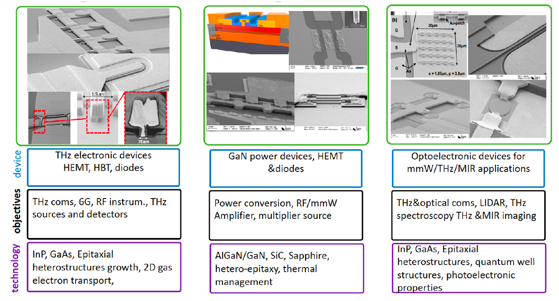
IEMN has a strong basis in design and fabrication of electronics devices based on III-V compound semiconductors. These devices are dedicated to improve the performances of the telecommunications systems in terms of energy efficiency, operation frequency or available power. In this context, IEMN is developping original ideas in order:
- to obtain InP/InGaAs HEMT and DHBT transistors with cut-off frequency beyond 1 THz for UHD telecom systems (low-noise and power amplifiers) but also InP UTC Photodiodes with improved efficiency and frequency limits for 1550 nm optical telecom systems and optical to THz telecom conversion.
- to improve the performances (efficiency, conversion loss, frequency band, etc) and the technology maturity (reaching TRL 5) of LTG-GaAs ultrafast optoelectronics devices for laser-based generation and detection of millimetre and THz waves. In this latter case, it covers the field of spectrum analysis for the characterization of THz devices and systems and the analog-to-digital conversion of millimetre waves.
- to develop AlGaN/GaN transistors for high power amplifier working in the millimeter waves spectrum for telecommunications (civil and military). GaN based Schottky diodes will be also studied to replace GaAs Schottky diode in electronics multiplication based THz sources, which are mainly based on the generation of harmonics of a low frequency source.
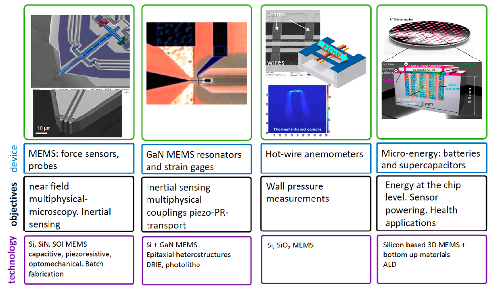
IEMN is pursuing MEMS-NEMS technologies already validated at low TRL scales (0-3). The objectives are to establish an efficient and industrial roadmap (TRL >4 then TRL >6). Several families of devices are envisaged:
- A first category includes MEMS/NEMS force transducers for near-field imaging or inertia. These devices target an operating frequency of >100 MHz combined with a resolution of < 1fN/Hz1/2
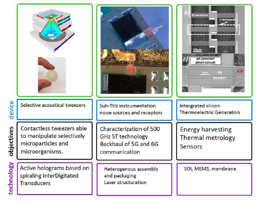
They are either all-Si or Si+GaN based, where GaN heterostructures enable electromechanical transduction and Si is used for 3D patterning of moving parts. This approach aims to provide hardened sensors for industrial IoT ; - sensors based on a glass/silicon/glass MEMS technology for instrumented opto-microfluidics cytometric systems. Here coupling 3D hydrodynamics, focusing and optical fiber access within the same chip will targets systems able to analyze and process in real time more than 6500 events per second.
- microbatteries and microsupercapacitors technologies that will be also at the basis of energy related applications.
Challenge 2: emerging technologies: new materials & physical concepts
Besides the continuous improvement of these existing technologies, IEMN will also work on devices based on rising materials and technologies or using original physical effects.
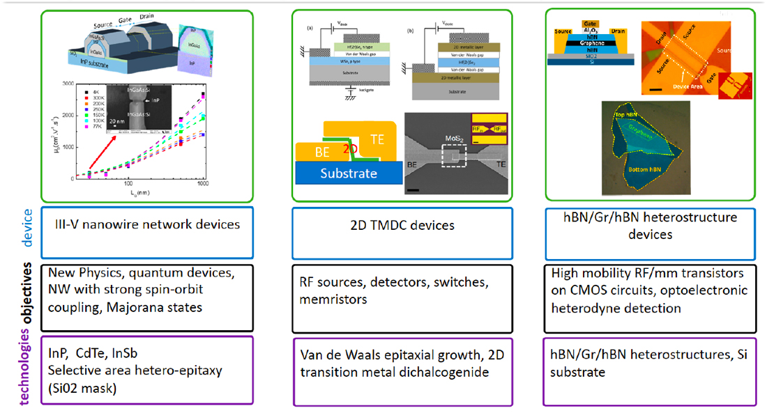
- IEMN investigates devices based on graphene-related-materials and two-dimensional metallic transitions materials (TMDC) for high-frequency electronics and optoelectronics applications. For example, we propose to study an ultrafast electronic switch overcoming the physical limits of the standard technologies by taking advantage of an ionic filament conduction mechanism observed in these materials.
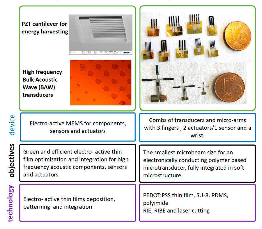
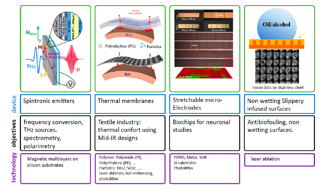
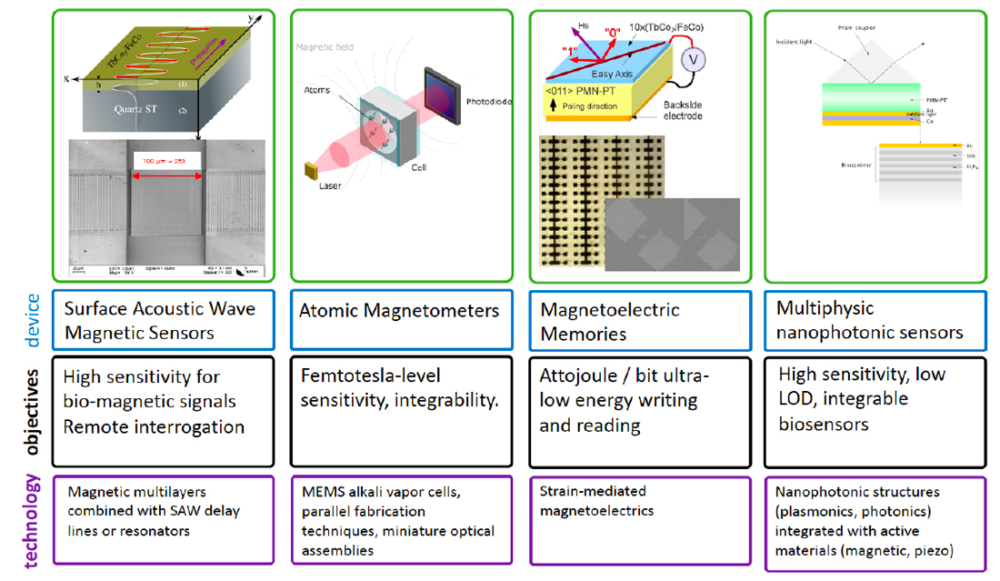
- The combination of magnetoelastic materials together with electro-active ones such as piezoelectrics or ferroelectric relaxors results in artificial multiferroic or magnetoelectric composites. IEMN develops devices where the possible control of magnetization in an energy efficient fashion which can be applied to memories or magnetic domain wall control, and devices where the magnetoelastic coupling can also be exploited in Surface Acoustic Wave devices. This topic involves theoretical studies of multiphysic phenomena as well as technological efforts to deposit, pattern and integrate these non-standard materials on wafers.
- We also work on magneto-plasmonic effects to obtain efficient THz/MIR isolators and Bio-sensors. In the former case, the idea consists in exploiting the magnetoplasmon cyclotron resonances in nanostructured low-effective mass materials (ex: InSb) to create non-reciprocal mirrors. In the second case the idea consists in using the non-reciprocal magneto-optical effects to design ultra-sensitive surface plasmon resonance sensors;
- In recent years, the rise of commercial QCL MIR lasers has opened up new possibilities in the MIR range (λ~ 2 µm-10 µm). Based on IEMN's expertise in designing and fabricating ultrafast optoelectronic devices in the IR range, we are developing ultrafast photoconductors in the MIR range using plasmonic nano-antennas to collect MIR radiation and AlGaAs/GaAs or InSb quantum well nanowires to perform the optoelectronic conversion.
- All optics ADC will also be studied by using a breakthrough concept in which an electro-optic polymer waveguide is combined with a microwave guide.
- We also plan to develop microsystems for high bandwidth bolometric detection of THz signals unlocking available detectors issues and able to work at room temperature, that will combine on chip silicon photonics to NEMS and microantennas.