Project ANR -21-CE24-0030
TUNNE2D
Miniaturizable tunnel diodes based on 2D materials
The information and communication society requires very high speed data transmission and processing networks, requiring high frequency (HF) components. Tunneling devices (TDs) are an essential building block, with potentially higher performance than thermionic devices. Indeed, inter-band tunneling carrier transport does not suffer from the limitations due to thermal activation and can lead to a negative differential resistance (NDR), a unique and differentiating feature for the development of HF sources and detectors. However, DTs are very sensitive to the chemical and electronic structure of the tunnel interface and their performance remains limited by the covalent nature of the bonds at the interface when fabricated using three-dimensional (3D) semiconductors such as Si, Ge or III-Vs.
In contrast, the absence of surface dangling bonds in two-dimensional transition metal dichalcogenides (DMTs) allows the formation of van der Waals (vdW) heterostructures without lattice adaptation and stress-free integration. One of the main objectives of the TUNNE2D project is to study the fabrication of vdW heterostructures without dangling bonds at the interfaces. Recent experimental results have confirmed the added value of DMTs for DTs governed by band-to-band tunneling. However, to date, these devices have been developed from exfoliated or transferred layers. These processes result in poor interface integrity and limited reliability and scalability.
This proposal aims to evaluate the capabilities of DMTs for tunneling devices. To this end, backward, Esaki and resonant tunneling diodes will be fabricated at wafer scale and fully characterized at low and high frequencies. The objectives are: (i) growth of layers and heterostructures of DMTs by chemical vapor deposition (CVD) and molecular beam epitaxy (MBE); (ii) comprehensive characterization of the layers and heterostructures, including interface properties and band alignment; (iii) design of tunnel diodes based on DFT calculations of material properties and quantum transport in the devices; iv) Fabrication of tunnel diodes; v) Comparison of DTs fabricated by CVD or EJM to provide the community with insight into the advantages/disadvantages of the two approaches; vi) Comparative evaluation of DMT-based diodes versus conventional 3D semiconductor-based diodes.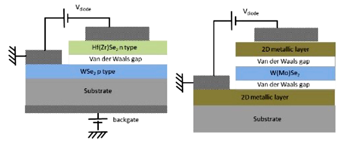
The project will focus on the family of Se-based DMTs offering the variety of materials required to fabricate these diodes, namely metallic, p-type and n-type semiconductor layers with different electronic affinities. Our approach is based on the strong interaction between the material aspects, the modeling and simulation and the electrical study of the devices. It gathers 3 academic partners (IEMN, CINTRA, C2N) with complementary skills and equipments in the elaboration and characterization of materials, fabrication and simulation of devices. IEMN has recently installed an EJM system entirely dedicated to the growth of DMTs and is expert in the development of 2D devices with advanced fabrication techniques. CINTRA is very active in the field of CVD growth of DMTs and has recently demonstrated the versatility of this technique for over 30 materials. C2N has a long history of tunneling device simulations and has recently focused on DMTs. The success of the consortium will build on both a long-term partnership of more than 10 years between IEMN and CINTRA and the long history of collaboration within IEMN and C2N projects.


