
| Typical job |
Post-doctoral position in fabrication and characterization of HEMT devices on ScAlN/GaN |
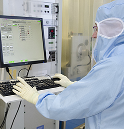
| Missions |  The recruited candidate will join the Microwave Components and Devices group (PUISSANCE) of the Institute
of Electronics, Microelectronics and Nanotechnology (IEMN). His mission will be to fabricate semiconductor
devices in the Institute's clean room. The candidate will work on different steps of the technological process
to fabricate devices which will then be characterized. The recruited candidate will join the Microwave Components and Devices group (PUISSANCE) of the Institute
of Electronics, Microelectronics and Nanotechnology (IEMN). His mission will be to fabricate semiconductor
devices in the Institute's clean room. The candidate will work on different steps of the technological process
to fabricate devices which will then be characterized. |
| Activities | The main activity will be to fabricate and characterize HEMTs (High Electron Mobility Transistors) on
ScAlN/GaN heterostructures, with the aim of going beyond the best performance currently achieved on GaN
HEMTs up to D-band. The material will be grown at CRHEA in Nice as part of a collaboration for the GaNEXT
project of excellence. At IEMN, the post-doctoral fellow will be involved in developing the technological
process to fabricate the devices in cleanroom, and characterizing them.
The various steps of the technological process will be developed and optimized, in particular :
The transistors will then be characterized with:
|
| Qualifications: | The candidate must have a phD degree in micro - nanotechnology, with knowledge of nanometric
components for microwave applications.
He should have good experience of cleanroom devices technology, and have successfully completed the various technological steps inherent in the fabrication of semiconductor devices. Skills in electrical characterization techniques will also be appreciated. |
| Context: | The candidate will join the PUISSANCE group at IEMN, which specializes in GaN-based components and devices for microwave power applications. This group has expertise in device simulation, characterization and technological manufacturing.
The candidate will work within the framework of the GaNEXT project of excellence. Most of the work will be carried out in clean room, but will also include measurements of the devices produced. The candidate will receive specific training in cleanroom safety and will be introduced to specific technological techniques for using the various resources available. |
Host Unit:
IEMN UMR CNRS 8520
Avenue Poincaré
59652 VILLENEUVE D'ASCQ CEDEX
www.iemn.fr
Contract Type:
Post-doctoral student (13 months)
Contact:
marie.lesecq@univ-lille.fr
Access to vacancies on the CNRS Employment portal :
https://emploi.cnrs.fr/Offres/CDD/UMR8520-MARLES0-003/Default.aspx


