IEMN
  • Home
  • News
    • IEMN Newsletters
    • M2-Ingé Internships
    • Job offers
    • All news
  • The Institute
    • Presentation
    • Organization of the institute
    • The Scientific Department
    • The Technological Department
    • Administrative and financial management
    • Rules of procedure
    • Our commitments
  • The Research
    • Scientific departments
      • Nanostructured Materials and Components
      • Micro / nano optoelectronics
      • Telecommunications Technologies and Intelligent Systems
      • Acoustic
    • Research groups
    • Flagship
  • Scientific Production
    • IEMN publications
    • Scientific production resources
  • The platforms
    • CMNF - Central Platform for Micro Nano Manufacturing
      • Engraving and implantation pole
      • In Line Analysis Unit
      • Soft Lithography and Bio Microfluidics
      • Deposits and epitaxy division
      • Lithography Unit
      • Packaging Division
      • CMNF Staff
    • PCMP - Multi-Physics Characterization Platform
      • Scanning Probe Microscopy Facility
      • Hyperfrequency, Optical and Photonic Characterization (CHOP)
      • Advanced Communications Systems and Prototyping cluster (SigmaCOM)
      • Characterisation, ElectroMagnetic Compatibility and Prototyping Centre (C2EM)
      • PCMP Staff
    • Services offered by our platforms
  • Partnership - Valuation
    • Academic Collaborations
    • ANR Projects
    • Main international collaborations
    • Industrial partnerships
    • The joint IEMN-Industry laboratories
    • Startups
  • Research Training
    • After the thesis
      • Do a post-doc at the IEMN
      • Towards the world of business and industry
      • Become a teacher-researcher
      • Become a Researcher
      • Starting a business at IEMN
      • FOCUS on a SATT engineer from the IEMN
    • A thesis at IEMN
      • Thesis and HDR defenses
      • Thesis topics
      • Financing
      • Doctoral studies
    • Master - Engineer
      • Masters ULille
        • Master Life Sciences and Technologies graduate programme
        • Master Nanosciences and Nanotechnologies - Speciality ETECH
        • Master Networks and Telecommunications
      • UPHF-INSA Masters
        • Master in Embedded Systems and Mobile Communications Engineering
        • Master Cyber Defense and Information Security
        • Master in Materials, Control and Safety
        • Master in Image and Sound Systems Engineering
      • Partner/Tutoring Engineering Schools
      • M2-Ingé Internships
    • The Lille branch of the GIP-CNFM
    • Nano-École Lille
  • Contact Us
    • Location
    • Contact form
    • Annuaire Intranet
  • Our support
  • fr_FR
  • Rechercher
  • Menu Menu
NEWS

Electronic lithography design engineer - External competition University of Lille

Typical job

B2D44 - Electronic lithography design engineer - CNRS external competition / Engineer in the development of thin film materials
https://data.enseignementsup-recherche.gouv.fr/pages/referens/

Missions

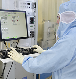
Ensuring the operation of electronic lithography equipment, as well as user training and support.

Activities
  • Co-managing two electronic lithography machines.
  • Provide training and support for users of this equipment.
  • Planning and controlling the use of equipment
  • Develop and qualify new electronic lithography processes.
  • Characterise electronic resins and lithographic results (reflectometry, ellipsometry, SEM, etc.)
  • Participate in internal and/or external research projects
  • Disseminate and promote lithographic processes (database, scientific articles, specialist networks, etc.).
  • Manage basic maintenance with remote assistance (hot line, remote) from the equipment manufacturer's engineers and/or manage their on-site intervention.
  • Drawing up specifications for the purchase or refurbishment of equipment, and formalising the purchasing and acceptance process, in conjunction with the administration.
  • Keeping a technological watch on materials used in electronic lithography (e.g. spray coater)
Qualifications: Knowledge

  • General knowledge of physics and engineering sciences.
  • In-depth knowledge of electronic lithography (management of proximity effects, CD) and its equipment.
  • In-depth knowledge of the resins used in electron lithography (contrast, sensitivity, influence of pre- and post-bake)
  •  In-depth knowledge of chemical developers
  • Basic knowledge of transverse micro- and nano-manufacturing processes (etching, deposition, characterisation).
  • Advanced knowledge of Linux, bash and python.
  • Vacuum techniques
  • Work in clean room
  • Health and safety rules
  • English language: B2 minimum

Operational skills

  • Using techniques associated with electronic lithography
  • Validate and control the conditions for electronic exposure
  • Analysing results
  • Troubleshooting equipment malfunctions
  • Applying equipment maintenance techniques
  • Use data processing software
  • Implementing a quality approach
  • Drawing up specifications
  • Write reports or technical documents
  • Making oral presentations
  • Keeping a scientific and technical watch

Behavioural skills

  • Ability to work independently and as part of a team
  • Ability to carry out bibliographical research
  • Initiative, analytical skills and thoroughness
Place of work Institute of Electronics, Microelectronics and Nanotechnology
(IEMN UMR 8520, University of Lille, UPHF, CNRS,) Centrale de Micro Nano Fabrication (CMNF,)
Lithography Centre, located at the IEMN Central Laboratory, avenue Poincaré, 59650 Villeneuve d'Ascq, France.
REGULATORY CONDITIONS : See article 26 of the decree no. 85-1534 of 31 December 1985

  • general conditions of access to the civil service (art. L321-1, L321-2 and L321-3 of the Code general civil service),
  • no age or nationality requirements
  • hold, on the date of the first test, a bachelor's degree or a diploma classified at least level 6 (formerly level II).
  • candidates who do not hold one of the required qualifications may apply for a equivalence for their professional experience. Application for equivalence is supplied with the application pack.


Host Unit:
IEMN UMR CNRS 8520
Avenue Poincaré
59652 VILLENEUVE D'ASCQ CEDEX
www.iemn.fr

Body :
Design Engineer / BAP B / Category A

Nature of the competition :
External

ONLINE REGISTRATION :
Registrations for the ITRF competitions will be open from Tuesday 02 April 2024 (12 noon, Paris time) to Tuesday 30 April 2024 (12 noon, Paris time).

For further information on the positionContact Yves DEBLOCK
Job: Head of Lithography Division CMNF
Mail : yves.deblock@iemn.fr

Assignee institution
University of Lille
Head of ITRF competitions: EMILIE VERMEULEN
Tel : 03 62 26 95 53
emilie.vermeulen@univ-lille.fr

Logo
Cité Scientifique
Avenue Henri Poincaré
CS 60069
59 652 Villeneuve d'Ascq Cedex, France
Tel : 03 20 19 79 79
CNRS Logo University of Lille Logo University Polytech Logo Junia Logo Centrale Lille Logo Renatech Logo RFnet Logo
Site map
Copyright Service ECM et pôle SISR 2024
  • Scientific production
  • Legal information
  • Privacy policy
Faire défiler vers le haut
fr_FR
fr_FR
en_GB
We use cookies to ensure you have the best experience on our website. If you continue to use this site, we will assume that you are happy with it.OKNoPrivacy policy