
Application and additional information:
| Missions |  Under the authority of the head of the Deposition and Epitaxy department, the agent will be responsible for ensuring the proper operation of the deposition equipment and the development of thin film materials. He/she will also be required to control and characterize the materials (thickness, roughness, structural analysis, chemical composition, stresses, electrical characterization, etc.). He/she will ensure the safety of the working environment related to the equipment (special gases, chemical precursors, gas treatment). He/she will work in collaboration with the technical staff of the pole and the research teams of the IEMN. Under the authority of the head of the Deposition and Epitaxy department, the agent will be responsible for ensuring the proper operation of the deposition equipment and the development of thin film materials. He/she will also be required to control and characterize the materials (thickness, roughness, structural analysis, chemical composition, stresses, electrical characterization, etc.). He/she will ensure the safety of the working environment related to the equipment (special gases, chemical precursors, gas treatment). He/she will work in collaboration with the technical staff of the pole and the research teams of the IEMN. |
| Activities | The agent's activity will consist in mastering, developing the know-how in thin film material deposition. This involves in particular:
|
Profile sought:
Operational skills:
Behavioral skills:
|
|
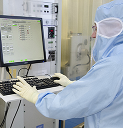
| Context: | Work in clean room |
Host Unit:
IEMN UMR CNRS 8520
Micro and Nano Manufacturing Center
Avenue Poincaré
59652 VILLENEUVE D'ASCQ CEDEX
www.iemn.fr
Nature of Job:
Job open to contractual employees only
Desired level of education:
Minimum 3 years of higher education in the field of materials chemistry.


