


Development of AlN/GaN HEMTs at IEMN
The increasing demand for bandwidth and data transmission speed for future applications such as 5G networks, satellite communications or radar requires the manufacturing of components delivering increased performance in the millimeter wave range. Silicon-based integrated circuits are limited to output powers in the order of a few watts up to Ka-band (26-40 GHz). Gallium nitride (GaN), in combination with a highly thermally conductive silicon carbide (SiC) substrate, offers significant advantages in power applications, such as a voltage withstand capability 5 to 10 times higher than traditional silicon or gallium arsenide based semiconductors, as well as improved heat dissipation. Nevertheless, the main limitations of this die are the power added efficiency (PAE) which defines the energy efficiency of the amplifiers, the control of trap effects which is essential in RADAR applications, as well as the reliability of transistors with reduced dimensions (ultra-short sub-150 nm gates). Researchers at IEMN in collaboration with SOITEC-Belgium have developed an approach offering the possibility of reducing the dimensions of GaN transistors while fully exploiting the potential of this emerging material. This work was supported by the Renatech network, the European Defense Agency (EUGANIC project) and the DGA/AID (French Ministry of Defence). The support of these partners enabled the acquisition of an expensive narrow-band power amplifier (40 GHz) delivering high power (> 10 W) as well as the associated elements (connectors, couplers, pulsed generators etc.). This important update makes the functionalities of this NVNA power bench at IEMN on this frequency band almost unique in Europe (i.e. high power active load pull type measurements in pulsed and CW regime).
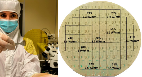
In this context, a specific heterostructure has been developed in order to overcome the technological bottlenecks in terms of reliability, exacerbated trap effects and efficiency for 100 nm gate GaN transistors operating at voltages higher than 15 V. This solution is based on the implementation of an ultra-thin AlN barrier layer. This layer with a thickness of less than 5 nm is favorable for frequency rise while delivering a high electron density. An SiN layer grown in-situ covers the barrier. It not only increases the robustness of the surface under strong electric field and/or temperature but also strongly reduces the effects of traps. Finally, the buffer layers have been designed to promote heat dissipation. The combination of these elements combined with an optimized manufacturing process has allowed to demonstrate unprecedented efficiencies of more than 70% at 40 GHz under high power density (> 5 W/mm). The absence of degradation during preliminary reliability measurements over a few tens of hours at different temperatures can also be noted. These results therefore open the way to a new range of millimeter wave power components, towards high efficiency power transistors in the millimeter wave range.
References
· GaN‐Based HEMTs for Millimeter‐wave Applications, Kathia Harrouche, and Farid Medjdoub, Chapter 3 from Nitride Semiconductor Technology: Power Electronics and Optoelectronic Devices book, https://doi.org/10.1002/9783527825264.ch3
· High Performance and Highly Robust AlN/GaN HEMTs for Millimeter-Wave Operation, K. Harrouche, R. Kabouche, E. Okada, and F. Medjdoub, IEEE J. of the Elec. Devices Soc. (7) https://doi.org/10.1109/JEDS.2019.2952314


