Probing noise at very high frequencies at the very heart of silicon
Discover a new type of electronic measuring probe that directly integrates a miniaturized noise source as close as possible to the contact tips. The objective is simple but the reality is complex: to characterize noise directly on silicon wafers, transistors, and BiCMOS circuits among the most frequency-performant, up to the G band of millimeter waves (140–220 GHz). In the absence of suitable solutions on the market, a customized amplified noise source was designed, with adjustable power, wide bandwidth, and built using the same technology as the components being measured. This original approach paves the way for more accurate, faster testing and active measurement probe technologies.
A smart measuring probe for very high frequencies: when the noise source enters the probe
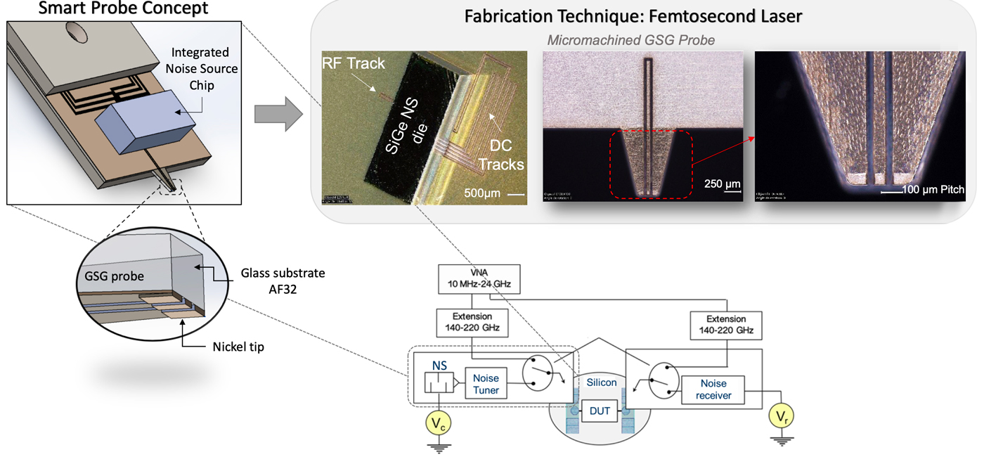
As communication, radar, and imaging systems move toward the upper end of the millimeter wave spectrum, microelectronic technologies must push their own limits. Designing a circuit capable of operating at 170, 200, or 220 GHz is one thing. Being able to measure it reliably is another, equally critical challenge. Without accurate characterization, there can be no simulation models and no robust applications. It is precisely this technological barrier that this project(1) conducted at the ST-IEMN(2) joint laboratory is tackling: integrating a noise source directly into the measurement probe, as close as possible to the contact tips with the silicon.
Active GSG measurement probe incorporating a G-band noise source (140-220 GHz) for wafer-level measurement
Why is noise a measurement tool?
In microwave electronics, noise is not just a nuisance: it is a reference signal. Engineers use it to determine key parameters such as the noise figure, which is used to evaluate signal degradation by a component (transistor, amplifier, mixer, etc.). At very high frequencies, these parameters directly determine the quality of an automotive radar, the range of a wireless link, or the sensitivity of an imaging sensor. However, in the G band (140–220 GHz), there are virtually no suitable commercial noise sources on the market: they are expensive, difficult to control, rarely flat in frequency, and above all difficult to interface with test benches dedicated to wafer-level measurement. As a result, characterizing a latest-generation transistor can sometimes be more complicated than designing it.
A decisive breakthrough: bringing the instrument closer to the device
Until now, two main approaches coexisted. The first consisted of integrating the test instrumentation directly into the chip to be measured (built-in self-test, or BIST). This was effective, but costly in terms of silicon surface area, and above all unusable for any technology other than the one in which it was manufactured. The second relied on external equipment connected by waveguides and transitions… all sources of loss, reflection, and uncertainty. The innovation introduced here is radical: placing the noise source in the measurement probe itself. Components are no longer tested “remotely,” but with an instrument almost attached to their terminal contacts. This approach introduces the concept of the smart probe, capable not only of contacting a circuit, but also of producing the noise spectrum necessary for its characterization.
An innovative noise source… using the same technology as the tested circuits
One of the project’s innovative choices was to design this noise source using the same technology as the components to be measured: STMicroelectronics’ (ST) B55X BiCMOS technology, capable of reaching cutoff frequencies above 400 GHz. The results are convincing: in a packaged configuration, adjustable excess noise levels of up to 29 dB are obtained between 140 and 170 GHz, with impedance matching better than –12 dB across the entire band. In other words: the noise source is powerful, controllable, and well-matched, where the market is silent.
The other key innovation: reinvented probe tips
High-precision measurement depends not only on electronics, but also on mechanics. At 200 GHz, a poorly aligned or overly fragile probe tip becomes a limiting factor. Hence the development of new Ground-Signal-Ground probes manufactured by femtosecond laser micro-machining. Made from a Schott AF32 glass substrate coated with nickel, these tips have remarkably low electrical contact resistance (0.05 ohms) and unmatched mechanical robustness: they can withstand forces more than three times greater than those required to ensure high-quality electrical contact. This advance is crucial for ensuring the reliability of thousands of successive contacts in industrial or laboratory environments.
A glass interposer to reduce losses
The final piece of the puzzle: the use of a glass interposer to integrate the ‘noise source’ chip as close as possible to the tips. Glass has low dielectric losses at very high frequencies, limiting signal attenuation and distortion. Thanks to laser micro-machining, interconnections are made with micrometric precision, simplifying the signal propagation path and drastically reducing parasitic transitions.
Benefits far beyond the laboratory
This work goes far beyond the performance of an experimental setup. It offers a new instrumentation model for millimeter wave technologies: more compact, closer to the component, and more universal. For manufacturers, this means reduced testing costs, faster technological maturity, and greater reliability of end products. For researchers, it means access to measurements that were extremely difficult to perform until recently. By bringing the instrument closer to the silicon to the physical limit, this “smart probe” revolutionizes the way instruments are used.
References
(1) Maya Alawar, Sylvie Lepilliet, Victor Fiorese, Sylvie Lépilliet, Daniel Gloria, Guillaume Ducournau, Emmanuel Dubois, ‘Toward smart probes for mmW on-wafer measurements: advanced packaging using laser micromachining of glass’, IEEE Transactions on Microwave Theory and Techniques, vol. 73, no. 11, pp. 8544-8555, Nov. 2025, doi: 10.1109/TMTT.2025.3595651
https://hal.science/hal-05214588 https://dx.doi.org/10.1109/TMTT.2025.3595651
(2) ST-IEMN Joint Laboratory – www.cnrs.fr/fr/actualite/laboratoire-commun-st-iemn-pascal-ancey-plus-de- vingt-ans-de-collaboration-dans-le Active GSG measurement probe incorporating a G-band noise source (140-220 GHz) for wafer-level measurement


