IEMN
  • Home
  • News
    • IEMN Newsletters
    • M2-Ingé Internships
    • Job offers
    • All news
  • The Institute
    • Presentation
    • Organization of the institute
    • The Scientific Department
    • The Technological Department
    • Administrative and financial management
    • Rules of procedure
    • Our commitments
  • The Research
    • Scientific departments
      • Nanostructured Materials and Components
      • Micro / nano optoelectronics
      • Telecommunications Technologies and Intelligent Systems
      • Acoustic
    • Research groups
    • Flagship
  • Scientific Production
    • IEMN publications
    • Scientific production resources
  • The platforms
    • CMNF - Central Platform for Micro Nano Manufacturing
      • Engraving and implantation pole
      • In Line Analysis Unit
      • Soft Lithography and Bio Microfluidics
      • Deposits and epitaxy division
      • Lithography Unit
      • Packaging Division
      • CMNF Staff
    • PCMP - Multi-Physics Characterization Platform
      • Scanning Probe Microscopy Facility
      • Hyperfrequency, Optical and Photonic Characterization (CHOP)
      • Advanced Communications Systems and Prototyping cluster (SigmaCOM)
      • Characterisation, ElectroMagnetic Compatibility and Prototyping Centre (C2EM)
      • PCMP Staff
    • Services offered by our platforms
  • Partnership - Valuation
    • Academic Collaborations
    • ANR Projects
    • Main international collaborations
    • Industrial partnerships
    • The joint IEMN-Industry laboratories
    • Startups
  • Research Training
    • After the thesis
      • Do a post-doc at the IEMN
      • Towards the world of business and industry
      • Become a teacher-researcher
      • Become a Researcher
      • Starting a business at IEMN
      • FOCUS on a SATT engineer from the IEMN
    • A thesis at IEMN
      • Thesis and HDR defenses
      • Thesis topics
      • Financing
      • Doctoral studies
    • Master - Engineer
      • Masters ULille
        • Master Life Sciences and Technologies graduate programme
        • Master Nanosciences and Nanotechnologies - Speciality ETECH
        • Master Networks and Telecommunications
      • UPHF-INSA Masters
        • Master in Embedded Systems and Mobile Communications Engineering
        • Master Cyber Defense and Information Security
        • Master in Materials, Control and Safety
        • Master in Image and Sound Systems Engineering
      • Partner/Tutoring Engineering Schools
      • M2-Ingé Internships
    • The Lille branch of the GIP-CNFM
    • Nano-École Lille
  • Contact Us
    • Location
    • Contact form
    • Annuaire Intranet
    • « Suivez-nous »
  • Our support
  • fr_FR
  • Rechercher
  • Menu Menu
RESEARCH at IEMN
Slide thumbnailRESEARCH at IEMN
RESEARCH at IEMN
RESEARCH at IEMN

Ultra-high-vacuum 3D printing for mesoscopic components

Very precise control of semiconductor crystals at the nanometer scale has become essential for the manufacture of advanced electronic components or for certain quantum technologies. In this context, nanowires based on III-V semiconductors with low electronic mass have particularly interesting properties. However, the fabrication of electronic circuits based on such objects requires their implementation in complex architectures (cross-networks) in a robust and reliable way while preserving their intrinsic properties.

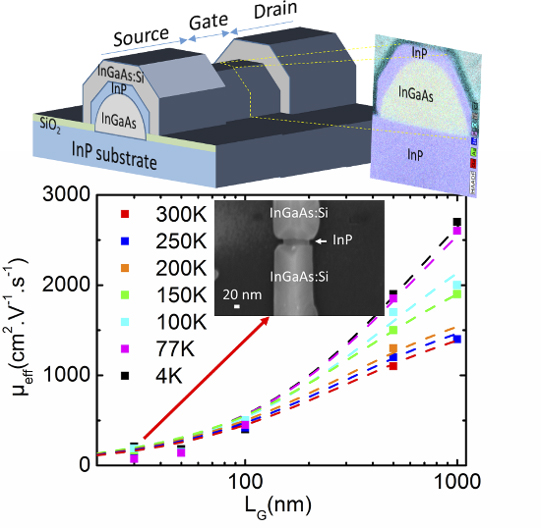
In this context, selective molecular beam epitaxy allows the elaboration of nanocrystals precisely localized on the substrate surface thanks to the use of a dielectric mask.  In this work*, we show how this growth method can be used to fabricate planar nanowires composed of an InGaAs core and an InP shell. A second step of selective growth also allows us to adorn these nanowires with highly doped contact zones to be able to fabricate transistors whose source/drain spacing can be adjusted down to less than 30 nm. With this bottom-up fabrication method, which avoids any semiconductor etching step, components with different lengths have been fabricated. They have made it possible to study the electron transport properties in nanowires down to very low temperatures in a transport regime where the electrons are likely to be ballistic.

* « Gate length dependent transport properties of in-plane core-shell nanowires with raised contacts », A.Bucamp, C.Coinon, D.Troadec, S.Lepilliet, G.Patriarche, X.Wallart and L.Desplanque, Nano Research 13, p61–66 (2020) https://doi.org/10.1007/s12274-019-2572-8

Logo
Cité Scientifique
Avenue Henri Poincaré
CS 60069
59 652 Villeneuve d'Ascq Cedex, France
Tel : 03 20 19 79 79
CNRS Logo University of Lille Logo University Polytech Logo Junia Logo Centrale Lille Logo Renatech Logo RFnet Logo
Site map
Copyright Service ECM et pôle SISR 2024
  • Scientific production
  • Legal information
  • Privacy policy
Faire défiler vers le haut
fr_FR
fr_FR
en_GB
We use cookies to ensure you have the best experience on our website. If you continue to use this site, we will assume that you are happy with it.OKNoPrivacy policy