IEMN
  • Home
  • News
    • IEMN Newsletters
    • M2-Ingé Internships
    • Job offers
    • All news
  • The Institute
    • Presentation
    • Organization of the institute
    • The Scientific Department
    • The Technological Department
    • Administrative and financial management
    • Rules of procedure
    • Our commitments
  • The Research
    • Scientific departments
      • Nanostructured Materials and Components
      • Micro / nano optoelectronics
      • Telecommunications Technologies and Intelligent Systems
      • Acoustic
    • Research groups
    • Flagship
  • Scientific Production
    • IEMN publications
    • Scientific production resources
  • The platforms
    • CMNF - Central Platform for Micro Nano Manufacturing
      • Engraving and implantation pole
      • In Line Analysis Unit
      • Soft Lithography and Bio Microfluidics
      • Deposits and epitaxy division
      • Lithography Unit
      • Packaging Division
      • CMNF Staff
    • PCMP - Multi-Physics Characterization Platform
      • Scanning Probe Microscopy Facility
      • Hyperfrequency, Optical and Photonic Characterization (CHOP)
      • Advanced Communications Systems and Prototyping cluster (SigmaCOM)
      • Characterisation, ElectroMagnetic Compatibility and Prototyping Centre (C2EM)
      • PCMP Staff
    • Services offered by our platforms
  • Partnership - Valuation
    • Academic Collaborations
    • ANR Projects
    • Main international collaborations
    • Industrial partnerships
    • The joint IEMN-Industry laboratories
    • Startups
  • Research Training
    • After the thesis
      • Do a post-doc at the IEMN
      • Towards the world of business and industry
      • Become a teacher-researcher
      • Become a Researcher
      • Starting a business at IEMN
      • FOCUS on a SATT engineer from the IEMN
    • A thesis at IEMN
      • Thesis and HDR defenses
      • Thesis topics
      • Financing
      • Doctoral studies
    • Master - Engineer
      • Masters ULille
        • Master Life Sciences and Technologies graduate programme
        • Master Nanosciences and Nanotechnologies - Speciality ETECH
        • Master Networks and Telecommunications
      • UPHF-INSA Masters
        • Master in Embedded Systems and Mobile Communications Engineering
        • Master Cyber Defense and Information Security
        • Master in Materials, Control and Safety
        • Master in Image and Sound Systems Engineering
      • Partner/Tutoring Engineering Schools
      • M2-Ingé Internships
    • The Lille branch of the GIP-CNFM
    • Nano-École Lille
  • Contact Us
    • Location
    • Contact form
    • Annuaire Intranet
  • Our support
  • fr_FR
  • Rechercher
  • Menu Menu
RESEARCH at IEMN
Slide thumbnailRESEARCH at IEMN
RESEARCH at IEMN
RESEARCH at IEMN

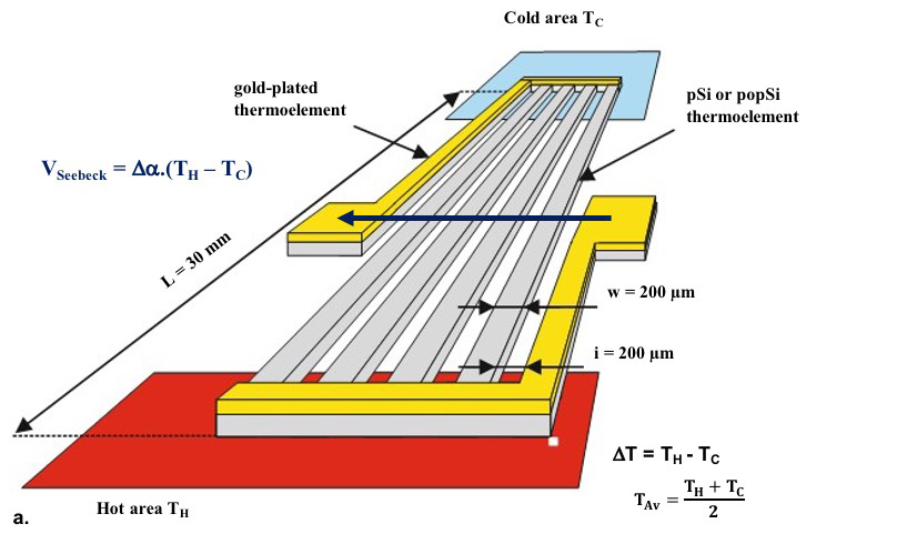
Elaboration and thermoelectric characterization of nanostructured polysilicon thin films by anodization


Over the last decade, the Internet of Things (IoT) market has grown almost exponentially. The energy issue has become one of the major challenges for IoTs but also, more broadly, for all microsystems. All innovative and environmentally friendly solutions to recover energy now play a strategic role in the development of these new technologies and are even the subject of increasingly important research and publications. The abundance of heat which represents energy in its most degraded form – all energy tends to become heat – gives a particular interest to thermoelectricity. For miniature applications, the thermoelectric effect (TE) has so far been exploited mainly in thermal sensors or in infrared detectors, where it favors high sensitivities despite low conversion efficiency.

The conversion efficiency of TE materials, used in conventional thermogenerators, is directly related to their dimensionless figure of merit (where is the electrical conductivity, a the thermoelectric power and the thermal conductivity of the TE material). These physical properties are oppositely dependent on carrier density and temperature, which complicates their performance optimization. The main avenues studied for the improvement of these materials use nanostructuring, in particular to reduce the phononic component of the thermal conductivity. The use of nanostructures, low dimensional systems or nano-composite structuring allows to confine the thermal transport of phonons in 2D or even quasi-1D.

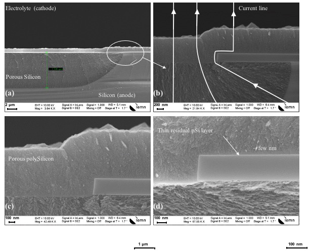
The work carried out at IEMN, in the field of thermoelectricity, has allowed the development of a new method to fabricate thin layers of nanostructured polysilicon, electrically isolated from their silicon substrate. Characterizations have shown that the porosification of polysilicon (POpSi) layers drastically reduces their thermal conductivity without impacting their thermoelectric power. This improvement of the thermal component overcompensates the degradation of the electrical conductivity and allows a 25 times increase of the figure of merit (for a POpSi layer with a porosity of 44%, ZT ~ 0.1). Simulations under COMSOL 3D® show that the integration of such layers in planar thermogenerators realized on suspended membranes (IEMN technologies) would allow a 30% increase of their conversion efficiency.

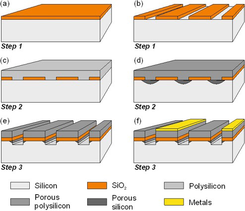
Flow chart of the porous polysilicon layer (a to d) and plated thermocouple strip (f)


Katir Ziouche, Ibrahim Bel-Hadj and Zahia Bougrioua
Nano Energy, 80 (2021) 105553, https://doi.org/10.1016/j.nanoen.2020.105553

katir.ziouche@univ-lille.fr
Logo
Cité Scientifique
Avenue Henri Poincaré
CS 60069
59 652 Villeneuve d'Ascq Cedex, France
Tel : 03 20 19 79 79
CNRS Logo University of Lille Logo University Polytech Logo Junia Logo Centrale Lille Logo Renatech Logo RFnet Logo
Site map
Copyright Service ECM et pôle SISR 2024
  • Scientific production
  • Legal information
  • Privacy policy
Faire défiler vers le haut
fr_FR
fr_FR
en_GB
We use cookies to ensure you have the best experience on our website. If you continue to use this site, we will assume that you are happy with it.OKNoPrivacy policy