
This work was initially part of the 2010-2013 State-Region Campus Ambient Intelligence Plan (CIA) and relates to the "Electrical Characterisation of Nano-Devices and Advanced Instrumentation (CENIA)" cross-cutting action. With the spectacular development of nano-objects, it was necessary to develop new means of electrical and electromagnetic characterisation on small scales. It was in this context that an EQUIPEX ExCELSiOR project (Experimental Centre for the Study of the Properties of Nanodevices in a Broad Spectrum from DC to Mid-Infrared) was led by the IEMN in 2012. The results obtained have enabled the laboratory to take part in several European H2020 EMPIR (European Metrology Programme for Innovation and Research - Euramet) projects bringing together the key players in microwave metrology in Europe.
Launched in December 2017, the European NMPB (Nanotechnologies, Advanced Materials, Biotechnology and Production) project entitled MMAMA led by IEMN and built with Keysight Technologies® (leader in microwave test and measurement equipment - Austria), METAS (Metrology Institute - Switzerland), Materia Nova® ASBL (Materials Research and Engineering Centre - Belgium), ETHZ (Swiss Federal Institute of Technology Zurich - Switzerland), QWED® (SME - microwave software and hardware solutions), Dracula Technologies® (SME - photovoltaic solutions), Adamant Composites® LTD (SME - nano-composite materials and structures), Ayming (monitoring and communication) aims to develop a unique microwave characterisation and modelling platform for advanced materials analysis for a broad community. The aim of this platform is to optimise the quality and manufacture of these materials/structures in an industrial context.
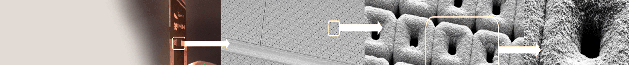
MMAMA focuses on the chemical industry, which offers a wide range of organic and non-organic nanoparticles for different sectors and applications. The quality and performance of the final product depend mainly on the chemical, electrical, optical and/or mechanical properties of these nanoparticles, as well as their arrangement on a macroscopic scale (amorphous, partially amorphous, hybrid/composite, multilayer). The same observation can be made for thin-film materials. The chemical constituents of a layered material are usually known, but the morphology, layer thickness and interface properties are crucial in determining the performance of the final product. Macroscopic characterisations are commonly used to verify properties on material surfaces. In this field of materials properties testing and characterisation, there is a 'gap' between the nano- and macro-worlds in terms of the types of instruments and testing methodologies and, incidentally, the types of data measured. On the one hand, in a laboratory context, local probe microscopy or scanning electron microscopy techniques enable resolutions of a few tens of nanometres to be achieved, but are destructive because of the preparation of the sample to be characterised. On the other hand, the resolution of measurement equipment for on-line testing is low, but the methods are fast and do not require any particular expertise.
The MMAMA project lies at the interface between laboratory characterisation at the nanometric scale and on-line characterisation at the macroscopic scale. The aim is to explore the link between the macroscopic electrical behaviour of thin-film materials and composites and their microscopic/nanoscopic properties. This link between macroscopic and microscopic electrical properties was explored by measuring the material using a range of microwave characterisation techniques at different dimensional scales.
The results obtained after three years are impressive. The MMAMA modelling and characterisation platform integrates innovative scanning near-field microscopy, active radar imaging, dielectric resonator and impedance spectroscopy techniques.
![]() Références :
Références :
Website : https://www.mmama.eu/
Linkedin : https://www.linkedin.com/in/mmama/
![]() https://www.youtube.com/watch?v=6s2hSd5muRE
https://www.youtube.com/watch?v=6s2hSd5muRE


