
Passive Resonant Sensors: Trends and Future Prospects
The choice of topic was « Passive Resonant Sensors: Trends and Future Prospects » [1]. The review focuses on technologies that exploit the « resonance phenomenon » that occurs with all types of waves: acoustic, electromagnetic and optical. The sensors considered include acoustic, magneto-elastic and electromagnetic transducers. They are presented through their relevant technological aspects and their main advantages, in particular their integrability in embedded systems and/or their energy autonomy requirement. The use of these resonant sensors is illustrated in a wide variety of applications (Fig. 1), ranging from environmental, structural, and food packaging monitoring, to wearable or implanted sensors of physiological parameters in health-related, Internet of Things (IoT), and Industry 4.0 applications.
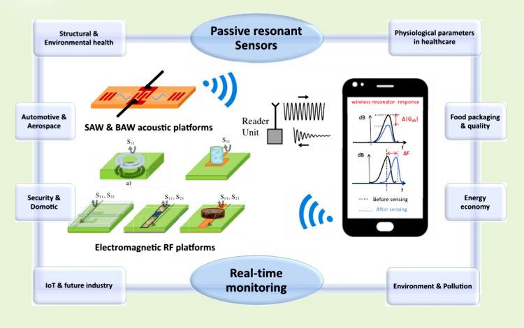
Fig 1. General scheme of the review article: Passive resonant sensors, designs and applications.
[1] H. Hallil et al., « Passive Resonant Sensors: Trends and Future Prospects, » in IEEE Sensors Journal, vol. 21, no. 11, pp. 12618-12632, 1 June, 2021, doi: 10.1109/JSEN.2021.3065734.
The AIMAN-FILMS group of IEMN has been working for more than fifteen years on the development of ultrasensitive sensor technologies allowing to push the limits of detection in terms of resolution. The review article highlights the main results obtained on magnetic field sensor technologies based on resonant MEMS exploiting magneto-electric coupling in composite structures based on magneto-elastic/piezoelectric thin films, magneto-elastic coupling in surface elastic waveguides functionalized by nano-structured magneto-elastic thin films. Temperature and stress sensors exploiting surface or guided elastic waves to allow operation in harsh environments. Sensors of physical or biochemical quantities exploiting a resonant cavity design based on the concept of phononic band gaps and the resulting quasi-flat defect modes.
1) Magnetic field sensor designs based on magnetoelectric and magneto-elastic effects have been proposed in 2007 and 2020.
Giant multi-physics couplings have been obtained in the vicinity of a critical state called Spin Reorientation Transition (SRT). A magnetoelectric coefficient of 40 V/(cm.Oe) was reported in 2007 using for the first time a Film/Film composite MEMS cantilever consisting of a nanostructured (FeCo-TbCo)n layer deposited on a piezoelectric aluminum nitride AlN layer [2].
In 2020, we proposed a magnetic field sensor design exploiting the interaction of a transverse surface wave with a nanostructured magnetoelastic thin film. The magneto-elastic layer allows guiding and confining the excited horizontal transverse surface wave to the surface of a piezoelectric substrate such as Quartz. This design achieves the intrinsic value of magnetic field sensitivity of a magneto-elastic thin film with a modulation of the order of 3% of the propagation velocity. This value defines the state of the art of magnetic field sensors based on the use of this detection mechanism [3].
These solutions are very promising for some medical diagnostic problems, especially those that exploit biomagnetic signals: magnetoencephalography (MEG) and magnetocardiography (MCG).
[2] Tiercelin et al., “Magnetoelectric effect near spin reorientation transition in giant magnetostrictive-aluminum nitride thin film structure,” Appl. Phys. Lett., vol. 93, no. 16, Oct. 2008, Art. no. 162902, doi:10.1063/1.3001601.
[3] A. Mazzamurroet al., “Giant magnetoelastic coupling in alove acoustic waveguide based onTbCo2/FeCo nanostructured film on ST-cut quartz”, Phys. Rev. Applied., vol. 13, no. 4, Apr. 2020, Art. no. 044001, doi:10.1103/PhysRevApplied.13.044001.
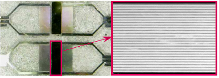
Fig 2. Horizontal shear surface wave’s devices functionalized with TbCo2/FeCo multilayered thin film (left). Scanning Transmission Electron Microscopy picture of the multilayered TbCo2/FeCo nanostructured thin film (overall thickness: 200 nm).
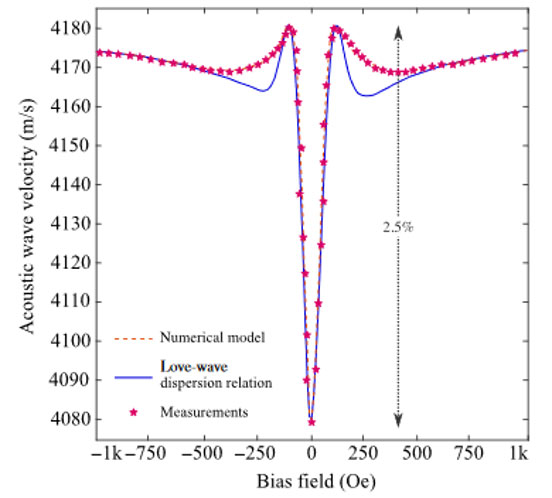
Fig 3. Giant magneto-elastic coupling 2.5% obtained with multilayered TbCo2/FeCo thin film combined to pure surface shear wave on quartz substrate at 1.2 GHz
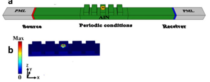
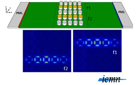
Fig. 4. a) Waveguide representation with cavity resonator made of nanomaterials as a cap layer.
b) Localized whispering gallery mode in the cap layer.
c) Demultiplexer design based on local resonance of cap layer.
[5] Moutaouekkil et al., “Highly confined radial contour modes in phononic crystal plate based on pillars with cap layers,” J. Appl. Phys., vol. 126, no. 5, Aug. 2019, Art. no. 055101;
[6] M Moutaouekkil al., Acoustic isolation of disc‐shaped modes using periodic corrugated plate‐based phononic crystal, Electronics Letters 54 (5), 2018, 301-303.
2) Acoustic wave resonators are very promising candidates for chemical and biological gravimetric detection.
In order to push the detection limit of current systems in terms of resolution, the AIMAN-FILMs group and the Ephoni team of the Physics group are collaborating to exploit the potential of phononic crystals and meta-materials for the design of MEMS resonators with minimal dissipation to the support structure and thus drastically improve the quality factor. Several designs exploiting surface or thin plate elastic modes in piezoelectric materials combined with a two-dimensional (2D) surface phononic crystal (SPnC) have been proposed. The SPnC consists of periodic mechanical resonators such as pillars or drilled holes. The proposed designs allow the realization of advanced functions based on the control of the elastic wave propagation: sub-wavelength confinement, wave guiding, demultiplexing function.
Among the proposed designs, the most promising are those exploiting the nearly flat defect modes located in the band gap of a phononic crystal. The designs highlighted here are proposed in the framework of Mohammed Moutaouekkil thesis of and have been the subject of two publications in 2018 and 2019 [4-5]. The phononic crystal is made of a micro-structured plate on the surface in the form of ribbons or pillars, which allows to obtain a wide band gap. The defect modes are introduced by depositing a nanometer thick gold disk on the surface of the ribbons or pillars.
These designs are very promising for the design of gravimetric sensors with a detection threshold up to attogram. Indeed, the design allows to confine the elastic wave at the nanometer scale and consequently reduce the mass of the resonator to make it comparable with the mass of the objects to be detected.
The SPnC can also be used to significantly slow down the speed of the acoustic waves based on local resonance phenomena and, consequently, limit the acoustic radiation towards the surrounding media, especially in case of contact with a liquid.


