 A large-scale two-dimensional material
for neuromorphic applications
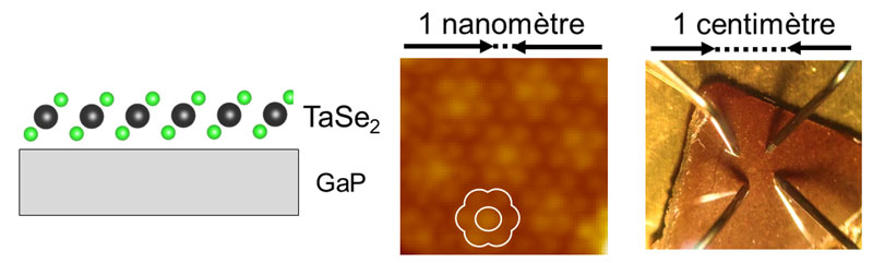
Mott materials are quantum materials whose resistive switching properties are analogous to the electrical response of biological neurons. A two-dimensional Mott material, TaSe2, recently discovered in its monolayer form, has been fabricated at IEMN by epitaxy on an industrial gallium phosphide (GaP) substrate. The electrical continuity of the monosheet has been demonstrated on a macroscopic scale, and the resistive switching property has been detected on a nanometric scale. This result opens up promising prospects for low-impact, energy-efficient electronics.
Quantum materials represent a broad class of materials in which strong electron interactions give rise to collective quantum electronic effects such as superconductivity, magnetism or resistive switching.
To enhance electronic interactions, we can typically use materials where the atoms have a large number of valence electrons (transition metals), or limit the dimensionality of the crystal to confine the electrons (2D materials, 1D materials, quantum dots).
The properties of quantum materials hold great potential for the development of innovative electronic components. In particular, electrical pulse-induced resistive switching in so-called Mott materials can mimic certain neuromorphic functions: the change in resistance state obtained following a series of electrical pulses is analogous to the response of a biological neuron [1].
One of today’s major challenges is to integrate these materials into the existing large-scale microelectronics industry, based on technologies specific to silicon substrates and III-V semiconductors such as GaAs and GaP. The challenge lies in both manufacturing and controlling the electronic properties of these materials on a large scale.
At the IEMN, an equipment dedicated to the synthesis of chalcogenide materials by molecular jet epitaxy, installed in 2020, has made it possible to fabricate layers of a two-dimensional Mott material discovered in 2021, 1T-TaSe2. Until now, this two-dimensional material, which is difficult to fabricate in crystalline form, had only been obtained on metal substrates. These substrates considerably reduce application possibilities, since they short-circuit the active material. Against this background, the EPIPHY group succeeded in fabricating TaSe2 monolayers on a III-V semiconductor substrate, gallium phosphide. These layers have been multi-scale characterized by the PHYSIQUE group.
Crystalline quality was confirmed by tunnel microscopy measurements. The expected crystal structure was observed, as was the charge density wave-like electronic modulation characteristic of this compound. In addition, a Moiré effect between the TaSe2 and the GaP substrate has been demonstrated, attesting to the fact that the layer is indeed a single layer of the material composed of a Ta atom between two Se atoms.
The Mott phase is at the origin of a bandgap of around one hundred millielectronvolts, which has been detected both at nanoscale by tunneling spectroscopy, and by cryogenic transport measurements. This study benefits from the acquisition in 2022 at IEMN of a cryogenic device enabling rapid characterization of electrical transport properties.
Generally speaking, it is currently difficult to obtain the extensive crystalline atomic layers required for industrialization. Monolayers of 1T-TaSe2 exhibit homogeneous electrical properties over several millimeters. Finally, we have observed the first signature of a resistive switching effect under the effect of an electric field, on a nanometric scale. These results [2] pave the way for the use of TaSe2 atomic layers in the large-scale production of ultra-compact neuromorphic components.
References
[1] Stoliar, P.; Tranchant, J.; Corraze, B.; Janod, E.; Besland, M.-P.; Tesler, F.; Rozenberg, M.; Cario, L. A Leaky-Integrate-and-Fire Neuron Analog Realized with a Mott Insulator. Adv. Funct. Mater. 2017, 27 (11), 1604740. https://doi.org/10.1002/adfm.201604740.
[2] Koussir, H.; Chernukha, Y.; Sthioul, C.; Haber, E.; Peric, N.; Biadala, L.; Capiod, P.; Berthe, M.; Lefebvre, I.; Wallart, X.; Grandidier, B.; Diener, P. Large-Area Epitaxial Mott Insulating 1T-TaSe2 Monolayer on GaP(111)B. Nano Lett. 2023. https://doi.org/10.1021/acs.nanolett.3c02813.
Website links:
https://www.iemn.fr/la-recherche/les-groupes/epiphy
https://www.iemn.fr/la-recherche/les-groupes/physique


