Projet ANR -23-CE51-0011
TWINS
Towards the co-integration of high frequency devices on epitaxial ScAlN
Vers la co-intégration de dispositifs haute fréquence sur ScAlN épitaxié
The communications network will undergo enormous changes in the coming years, with the surge in data traffic for mobile telecommunications and the emergence of the Internet of Things. The need to meet this demand calls for monolithic device integration to reduce costs and circuit size, while increasing functionality and performance. The 1-10 GHz frequency range, of great interest for telecommunications including beyond 7 GHz for future 6G, requires the development of high crystalline quality materials such as nitrides for the development of critical elements such as power amplifiers. ScAlN is currently considered the most promising barrier-zone material for the next generation of RF HEMTs (high electron mobility transistors), replacing AlGaN or AlN materials due to its high carrier density and mobility. In addition, thick ScAlN is currently used as a piezoelectric material for surface acoustic wave (SAW) devices, although their performance is currently limited by the crystalline quality of the sputtered materials. These devices will therefore be able to benefit from the advantages of epitaxial ScAlN with improved crystalline quality, all the more so for operation in the 1-10 GHz frequency range.
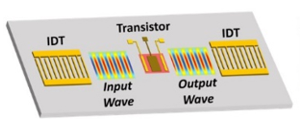
Against this backdrop, the ambition of the TWINS project is to demonstrate the potential of epitaxial ScAlN for fabricating high-performance RF devices, and to provide an insight into the technological avenues for their monolithic co-integration on the same substrate. This will enable the development of a monolithic, voltage-controlled oscillator operating in the 1-10GHz range, based on the joint use of SAW devices and transistors. ScAlN will be grown by molecular jet epitaxy to achieve high crystal quality. The elementary devices required for the targeted application (SAW and transistors) will be the subject of specific growth technology development. Finally, the possibility of using localized epitaxy will be investigated to benefit from the optimization of the individual structure on the same substrate in order to co-integrate the two devices.


