


 Rewarding excellence, innovation and success
La compagnie ALLOS semiconductors s’est vu décerner un CS Award portant sur des travaux effectués en étroite collaboration avec l’équipe de recherche du Dr Farid Medjdoub de l‘Institut d’électronique, de microélectronique et de nanotechnologie. Les derniers résultats de l’IEMN démontrent notamment une tension de claquage de plus de 1400 V pour les mesures verticales et latérales sur le prochain produit d’ALLOS, l’épiwafer GaN-on-Si pour les appareils de 1200 V.

By Alain Léger
Director of Research at the CNRS
Contact: leger@lma.cnrs-mrs.fr
Wednesday 28 March 2018 at 14:00
IEMN Ampli LCI - Villeneuve d'Ascq
Abstract:
This talk will present some aspects, first introductory, then more recent, of non-regular mechanics. A number of situations, edge conditions or behaviour laws provide examples of non-regularity in mechanics. We will concentrate mainly on the case of contact and friction, but several fundamental aspects would be identical in the cases of plasticity, damage, etc. In all cases, the introduction of non-regular conditions in continuum mechanics leads to open and difficult mathematical problems. To this end, an attempt will be made to give a detailed account of the current state of affairs, in the form of a list of problems that have been solved or are still open, so as to clarify the situations in which it is legitimate or not to use results from different areas of physics, and it will be observed that it is in these cases simple models which, provided they are well chosen, provide qualitative information where models closer to physics would be inaccessible.
It will be recalled that non-regularity removes the possibility of referring to the classical framework of the theory of differential equations or partial derivatives. After a few results, stated in the case of a very simple mechanical system but generalisable to all discrete problems, a large part of the presentation will be devoted to the study of the response to a periodic load, as is traditional in the qualitative study of dynamic systems.
Initially, the mechanical system will be linear, which will make the results usable qualitatively in many areas of physics, acoustics or vibrations. Particular attention will be paid to the transition between zones of different behaviour, and it should be noted that no transition to chaos is observed when the only non-linearity is due to contact and friction. We will then add a regular non-linearity of the large deformation type. We will then see that the response can include zones of non-periodic behaviour, which will lead us to question the coupling between different types of non-linearity.
Link to the website http://www2.cnrs.fr/presse/communique/5493.htm

Sabine Szunerits (à gauche) et Anne-Christine Hladky (à droite) ©Joaquim Dassonville
Comme chaque année, le Centre National de la Recherche Scientifique décerne la médaille d’argent afin de distinguer des chercheur.e.s pour l’originalité, la qualité et l’importance de leurs travaux, reconnus sur le plan national et international.
Parmi les vingt lauréat.e.s de l’année 2018 figure deux chercheures de l’IEMN (UMR 8520 – CNRS/Université de Lille/ISEN/UVHC/Centrale Lille) :
Sabine Szunerits, Spécialiste des biocapteurs et de la nano-médecine pour le traitement des infections virales et bactériennes ou l’hypothermie.
Professeure des Universités exerçant au sein du Département de Chimie de l’Université de Lille et au sein du groupe NanoBiointerface de l’IEMN a été distinguée par l’Institut de Chimie – INC.
Anne-Christine Hladky, Experte en métamatériaux acoustiques.
Directrice de Recherche au CNRS et responsable du groupe ACOUSTIQUE de l’IEMN a été distinguée par l’Institut des Sciences de l’Ingénierie et des Systèmes – INSIS.
Téléchargez le communique de Presse CNRS

HORIBA JOBIN YVON et l’Institut d’Electronique de Microélectronique et de Nanotechnologie (IEMN-CNRS) s’associent et créent une « équipe mixte » de recherche visant à développer des outils de caractérisation innovants ainsi que la caractérisation physico-chimique de nanomatériaux. Cette structure, financée par des crédits FEDER de la Région Hauts-de-France, soutient des actions de recherche engagées depuis 2012, notamment sur la fabrication de sondes micro-nano-fabriquées pour applications à la spectroscopie Raman dont HORIBA JOBIN YVON est leader mondial
La thématique de recherche de l’équipe mixte concernera le développement d’outils de caractérisation innovants ainsi que la caractérisation physico-chimique de nanomatériaux par techniques de microscopie à force atomique et de spectroscopie Raman et infrarouge à exaltation de pointe. Le travail portera à la fois sur le design et fabrication de nouvelles générations de sondes de microscopie champ proche par techniques de micro et nano-fabrication, et un travail de nano-caractérisation avancée de propriétés physico-chimiques de matériaux nouveaux.
References
HORIBA JOBIN YVON est l’un des plus importants fabricants de systèmes et composants de spectroscopie et d’analyses. L’entreprise est leader mondial en spectroscopie Raman. Elle conçoit et fabrique à Villeneuve d’Ascq des appareils à la pointe de la technologie depuis plus de 50 ans. Les équipes de R&D et du laboratoire d’applications HORIBA Villeneuve d’Ascq travaillent actuellement sur le « nano-Raman », technique exploitant l’effet d’exaltation de pointe (« Tip Enhanced Raman Spectroscopy » ou TERS) et qui permet d’apporter à la spectroscopie Raman la résolution spatiale nanométrique des techniques de microscopie champ proche comme la microscopie à force atomique. http://www.horiba.com/fr/
L’IEMN (UMR8520, CNRS – Université de Lille – Université de Valenciennes et du Hainaut-Cambrésis – Centrale Lille et ISEN-yncréa) a une expertise reconnue internationalement en micro et nano-fabrication (l’IEMN est membre du réseau RENATECH), ainsi qu’en microscopie champ proche. L’IEMN a été lauréat en 2012 d’un PIA EQUIPEX Excelsior (www.excelsior-ncc.eu) couplant la microscopie champ proche aux excitations électriques et/ou optiques du continu au THz. Dans ce contexte, l’IEMN a développé des actions de recherche couplant microscopie champ proche et optique (par exemple SNOM infrarouge ou Terahertz, micro et nano-fabrication de cantilevers), et engagé une activité de recherche en convergence avec les applications visées par la société HORIBA.
Contacts
Researcher l Thierry Mélin l T 04 32 50 06 59 l thierry.melin@univ-lille1.fr
Presse CNRS l Stéphanie Barbez l T 03 20 12 28 18l stephanie.barbez@cnrs.fr
Presse Université de Lille l Cristelle Fontaine l T 03 20 96 52 57l cristelle.fontaine@univ-lille2.fr


L’explosion des réseaux sans fil pousse les technologies actuelles dans leurs retranchements. Si les fréquences térahertz offrent les débits nécessaires pour y pallier, elles manquent encore de composants adaptés. Des chercheurs de l’IEMN et de la Brown University de Providence ont donc conçu et testé le premier système mux/demux fonctionnant à ces fréquences. Cet élément permet de « zapper » entre différents flux et d’atteindre un débit mille fois supérieur au Wi-Fi. Ces travaux sont publiés dans la revue Nature Communications.
Les réseaux sans fil actuels utilisent des micro-ondes de la gamme hyperfréquence, comprises entre 1 et 100 GHz. Comme les vitesses de transmission des données dépasseront dans quelques années les capacités de nos réseaux, le monde de la recherche se penche désormais sur les ondes térahertz1. Grâce à leurs fréquences plus élevées que les micro-ondes, elles atteignent de meilleurs débits. Ces ondes nécessitent cependant d’adapter et de rendre compatible toute l’électronique consacrée aux télécommunications. Des chercheurs de l’Institut d’électronique, de microélectronique et de nanotechnologie (IEMN, CNRS/Université Lille 1/ISEN Lille/Université de Valenciennes/École Centrale de Lille) et de l’université américaine Brown ont mis au point le premier système de multiplexage et de démultiplexage térahertz.
Grâce à un mux/demux, plusieurs signaux transitent à travers un seul canal de communication et se séparent ensuite à volonté. Ce composant essentiel permet par exemple de transporter plusieurs chaînes de télévision à la fois, ou de connecter des centaines d’utilisateurs sur un même réseau Wi-Fi. Les chercheurs ont ici utilisé deux plaques métalliques parallèles afin de guider les ondes THz. Une fente coupée laisse une partie des ondes s’échapper avec un angle lié à leur fréquence, ce qui les isole et les trie. Le débit total de données démultiplexées a ainsi pu atteindre 50 Gbit/s dans la bande 300 GHz, soit environ 1000 fois celui d’un réseau Wi-Fi standard (54 Mbit/s).
Ces travaux ont été réalisés dans le cadre de la fondation I-site Université de Lille Nord Europe, au sein du Hub « Human-Friendly Digital World ». Ils ont été soutenus par l’ANR, l’Université de Lille, l’IEMN, le CNRS, RENATECH, PIA Equipex : FLUX (Fibres optiques pour les hauts flux), le projet ExCELSiOR, le conseil régional Nord-Pas de Calais, le FEDER et le CPER « Photonics for Society ».
1 1 GHz = 109 hertz ; 1 THz = 1 000 GHz
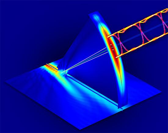
© IEMN
Démultiplexeur orientant dans l’espace le signal télécom THz (bande 300 GHz)
Frequency-division multiplexer and demultiplexer for terahertz wireless links
J. Ma, N. J. Karl, S. Bretin, G. Ducournau & D. M. Mittleman
Nature Communications 8, Article number: 729 (2017)
DOI :10.1038/s41467-017-00877-x
https://www.nature.com/articles/s41467-017-00877-x
Researcher contact :
Guillaume Ducournau – IEMN
INSIS communication contact :
insis.communication@cnrs.fr

Jing Li
Jing Li
Institut Néel, CNRS and Grenoble Alpes University
Equipe : Théorie de la matière condensée
Tuesday, October 24th 11.30 am/ Salle du conseil LCI
Abstract:
The description of the electronic and optical properties of complex supramolecular systems such as
those of interest in organic electronics represents a severe challenge for first principles techniques,
owing to the large molecular dimensions and to the ubiquitous presence of disorder. We will report
on our original hybrid QM/MM scheme merging many-body perturbation theory (GW formalism
and Bethe-Salpeter equation) with accurate classical polarizable models of atomistic resolution. Our
results for bulk pentacene prove that the gap is insensitive to the partitioning of molecules in QM
an![]() d MM subsystems, as a result of the mutual compensation of quantum and classical
d MM subsystems, as a result of the mutual compensation of quantum and classical
polarizabilities, clarifying the relation between polarization energy and charge delocalization. Our
embedded GW calculations, are capable to accurately describe ionization energies and electron
affinities at crystal surfaces of penatcene and perfluoropentacene from first principles.
The electronic and optical properties of the paradigmatic F4TCNQ-doped pentacene in the lowdoping
limit are investigated by a combination of state-of-the-art GW and Berthe-Salpeter manybody
ab initio methods accounting for environmental screening effects, and a carefully
parametrized model Hamiltonian. We demonstrate that while the acceptor level lies very deep in the
gap, the inclusion of electron-hole interactions strongly stabilizes dopant-semiconductor charge
transfer states and, together with spin statistics and structural relaxation effects, rationalize the
possibility for room-temperature dopant ionization. Our findings reconcile available experimental
data, shedding light on the partial vs. full charge transfer scenario discussed in the literature, and
question the relevance of the standard classification in shallow or deep impurity levels prevailing
for inorganic semiconductors.
References :
J. Li, G. D’Avino, I. Duchemin, D. Beljonne, X. Blase, J. Phys. Chem. Lett. 7, 2814 (2016)
J. Li, G. D’Avino, A. Pershin, D. Jacquemin , I. Duchemin, D. Beljonne, X. Blase, Phys. Rev.
Materials, 1, 025602 (2017)

Amin Arbabian
Assistant Professor, Department of Electrical Engineering
Stanford University
Wednesday, October 18th 5.30 pm / Amphi Jean Noël Decarpigny, ISEN Lille
Abstract:
Advances in healthcare technologies have mainly focused on therapeutics, interventional procedures, and “late-stage” diagnostics. These steps have undergone significant improvements, leading to higher survival rates and enhancements in quality of life. Nevertheless, current trends are unsustainable due to the inadequate outcomes on specific critical diseases and skyrocketing national healthcare costs. An important example is cancer, where mortality rates have not seen major improvements, even with the tremendous technological advances in diagnostic imaging tools over the last four decades.
In this talk I will outline our efforts in better marrying technology and healthcare with new systems that 1) enable continuous “Nyquist” imaging and screening to enable preventive/predictive care, and 2) introduce smart implants for precision monitoring and closed-loop therapies. Preventive screening through continuous monitoring has the potential to fundamentally revamp our understanding of disease as well as targeted therapy. Today, the human body is monitored infrequently, perhaps on an annual basis and with a low “resolution”. This is in contrast with advanced electronic systems (many of which our community designs and ships), which are frequently monitored and calibrated. I will summarize a few example projects that aim to address these issues, including portable, semiconductor-based, “Tricorder” imaging systems, ultrasound-powered implantable devices that can measure, detect, and act upon local physiological changes through closed-loop neuromodulation or “electroceuticals”, and finally our new investigation of a noninvasive methods of neuromodulation based on ultrasonic excitation.
Short Bio:
Amin Arbabian received his Ph.D. degree in EECS from UC Berkeley in 2011 and in 2012 joined Stanford University, as an Assistant Professor of Electrical Engineering. His research interests are in mm-wave and high-frequency circuits and systems, imaging technologies, and ultra-low power sensors and implantable devices. Prof. Arbabian currently serves on the steering committee of RFIC, the technical program committees of RFIC and ESSCIRC, and as associate editor of the IEEE Solid-State Circuits Letters (SSC-L) and the IEEE Journal of Electromagnetics, RF and Microwaves in Medicine and Biology (J-ERM). He is the recipient or co-recipient of the 2016 Stanford University Tau Beta Pi Award for Excellence in Undergraduate Teaching, 2015 NSF CAREER award, 2014 DARPA Young Faculty Award (YFA) including the Director’s Fellowship in 2016, 2013 Hellman faculty scholarship, and best paper awards from several conferences including ISSCC (2010), VLSI Circuits (2014), RFIC symposium (2nd place, 2008 and 2011), ICUWB (2013), PIERS (2015), and the MTT-S BioWireless symposium (2016).